Bride of Zen
Nelson Pass
Introduction
This is the second installment of a trilogy of construction projects centered around the performance obtainable from absolutely minimalist circuitry. Part one described the Zen amplifier, a 10 watt single-ended class A power amplifier using a single MOSFET gain stage. In this piece we will examine its preamplifying mate, also a single gain stage MOSFET circuit.
A lot of what I might say about this design has already been expressed in the Zen amplifier piece, and will not be repeated here. It is enough to say that I continue to be very intrigued by the sound of very simple topologies, single-ended in particular, and the use of MOSFET gain devices in realizing them. I assert that simpler circuits sound better. Anyone who disagrees is welcome to that opinion, and I wish them well listening to op amps.
As with the Zen amplifier, the purpose here is to explore a design which pushes simplicity to the limit. I want you to build it and experience not only the satisfaction of creating something tangible and functional, but also the pleasure of subjectively high performance audio.
As before, the simplest possible gain circuit has one stage, with a single transistor. Of necessity for linear operation, it must be operated in single-ended class A, and because we want both a high input impedance and voltage gain, the only useful connection is common-source, where the input signal is presented to the Gate of the MOSFET, and the output signal appears at the Drain.
Quite a few people have told me that they understood the concept of single-ended Triode amplifiers, and had not imagined that such a thing could be done with transistors. Conceptually, you can do almost anything with transistors that you could with tubes, although you do not always get the same results. The converse will not be true until a reliable supply of positrons becomes available to run through a P channel tube.
I did not find it practical to build a single gain stage tube amplifier, but the relaxed conditions under which a preamp functions makes a tube version of this circuit workable. Simply adjust the voltage and bias values for a tube instead of the MOSFET we will use here. I leave that as an exercise for the reader.
Requirements
Due to its extreme simplicity, the Zen amplifier’s interfaced needs to be indulged a bit, both at the output and also at the input. With respect to its output, it is designed for an 8 ohm load with an efficiency of 94 dB or greater. I have driven the Zen into Thiel 3.6 loudspeakers, 88 dB efficient at 2.3 ohms, but the result is not pretty. With a pair of Klipsch speakers it will throw off its mild mannered disguise and behave like a party animal.
The Zen amp input makes a preamp do a little more work than usual. Depending on the specific input values, its input impedance is typically 4.75 KOhm, and it needs about 2.5 volts input to drive it to full output. Its gain is about 15 dB, which is 10 dB less than most power amps and it requires more signal from the preamp for equivalent levels.
The point of a preamp circuit here is to function as a gain circuit with a high input impedance, a low output impedance, and a volume control. This preamp has a 50 KOhm input impedance, variable gain to about 15 dB, and will deliver the 2.5 volts at .1% distortion or less.
In the Zen amplifier, the need to linearly swing a relatively large amount of current into a load of varying impedance gave us a good reason to employ negative feedback around the MOSFET. Without it, the damping factor would be extremely low, and any impedance variation in the loudspeaker would give a large variation in frequency response.
The Zen preamp circuit has a much easier job in this regard, as the load attached to the Drain of the MOSFET will be resistive over the audio frequency range, allowing for intrinsically flat response. We will have much less reason to employ feedback in this circuit, and so we will not.
Another advantage that the preamp circuit will enjoy over the power amplifier is the relatively small dissipation involved. The Zen single-ended power amplifier idles at more than four times its output rating, typically 50 to 60 watts. The Bride of Zen will not typically be asked to deliver more than a milliwatt, but the MOSFET will have no difficulty dissipating a watt or so. This will allow us to bias the transistor at very much higher voltages and currents than are required to drive the load, enormously enhancing the performance.
A single common-source gain device will invert the phase of the signal it amplifies, and this must be taken into account when using the circuit in an audio system. The Zen amplifier also does this, but we reversed the phase on its output terminals to compensate, which is not possible here. Using the Zen preamp usually requires that we adjust the phase of connection between amplifier and loudspeaker for phase integrity.
The importance of proper absolute phase has been discussed elsewhere, including the original Zen amplifier contribution. I will simply say that proper absolute phase is a legitimate factor in the overall quality of sound reproduction. Even if I could not hear phase reversal, aesthetic considerations alone would prompt me to assure that it was correct.
Volume Control
We will place the volume control at the output of the circuit, giving us a higher output impedance than is typical. Depending on the position of the volume control, the output impedance will range from 0 to 1.5 KOhms.
Normally you see the volume control potentiometer at the input to the preamp circuit, and in this way you can insure that the input will not be overloaded. Placing the potentiometer at the output has two advantages, however, the first being that all circuit noise will be attenuated as the volume setting is reduced. Placing the volume control at the output allows the input of the gain stage to look directly at the source. This improves the bandwidth and distortion of the circuit by providing a lower RC figure for the input capacitance of the MOSFET. If you desire to place a potentiometer at the input of the circuit, feel free to do so before the input coupling capacitor in place of R107.
Because the input to the Zen amplifier is a resistor operating into a virtual ground summing junction, it is insensitive to a resistive source impedance. The gain of the amplifier will alter by the addition of the source resistance, but the distortion and bandwidth performance will not change appreciably. A circuit driving the Zen amplifier need not have a particularly low output impedance, as long as it is resistive in character.
Is a maximum 1.5 KOhm source impedance a problem? Not in my experience, as long as it is passive in character, as in the case of this circuit which has no feedback. You could conceivably see some rolloff at the top end, but even 1000 pF loading will only take the bandwidth down to 100 KHz.
The Schematic
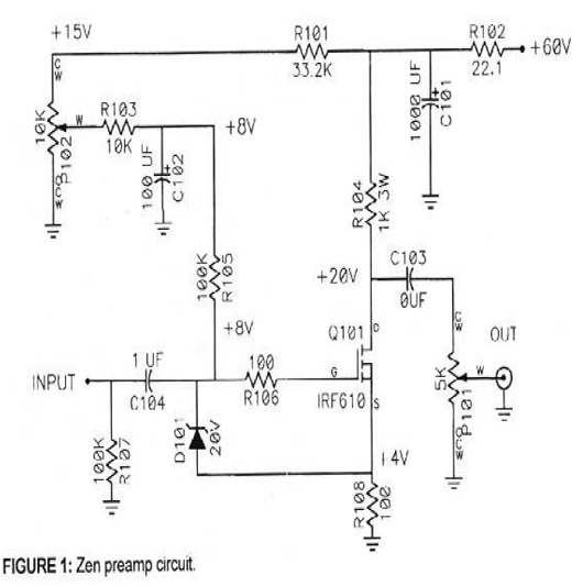
Figure 1 shows the schematic of the one channel of the Zen preamp. There is one transistor, Q101, and N channel power MOSFET. Input signal is presented to the gate of the MOSFET and the output is taken from the Drain. Everything else in the circuit is used to bias up the MOSFET appropriately.
While not necessarily true of all MOSFET devices, the types we will be considering perform better at higher supply voltages and higher currents. To take advantage of this, we will use a relatively high voltage supply at 60 volts and will bias the gain device at 40 milliamps.
We will provide approximately +7.5 DC volts to the gate of the MOSFET in order to turn it on. The MOSFET will require about 3.5 volts Gate to Source voltage to conduct the 40 milliamps, and this will leave 4 volts left over to be placed across the 100 ohm resistor, R108, which gives us 40 milliamps of current through Q101.
The DC input bias is delivered by the components R101, P102, R103, R105, and C102. The positive supply voltage is divided down by R101 and P102, and can be adjusted by P102. R103 and C102 provide noise filtering, and the adjusted quiet DC voltage is connected to the input through R105. To keep the source impedance from altering the DC bias, we capacitively couple the input through C104, which is a 1 uF film capacitor. The RC network of C104 and R105 produces a high pass characteristic at the input which is 1.6 Hz.
R107 is an optional part which is used to prevent transients when the input selector is switched. R106 is a 100 ohm nominal resistor used to prevent parasitic oscillations in the MOSFET. D101 is a zener diode which serves to protect the Gate of the MOSFET from voltages in excess of the 20 volt Gate-to-Source rating.
Signal input at the gate of the MOSFET causes the current through the transistor to vary, producing output AC voltage across R104. The gain of the circuit is the ratio of the output loading divided by the apparent resistance formed by the 100 ohm R108 and the inverse of the transconductance of the MOSFET. At this current with typical devices, that value is about 110 ohms total. At audio frequencies the output load is the 1000 ohms of R104 in parallel with the combination of output potentiometer P101 (the output level control) and the load. This value is always less than 800 ohms, so the gain of the circuit is somewhat less than 8 without an external load.
The 40 milliamps of DC current flowing through Q101 sets up a drop of 40 volts across R104, leaving about 20 volts DC at the Drain of Q101. Since we do not want to pass this along to the amplifier, we use output coupling capacitor C103, which rolls off the output below 3 Hz without an output load.
The circuit will use a regulated power supply, but since any noise on the supply will appear at the output through R104, it is desirable to clean in up as much as possible. R102 and C101 form a passive filter at the supply line to perform this task.
Referencing Fig. 1, note that the component numbers of one channel begin with 100, and the components of the other channel begin with 200. The power supply will have numbers which begin with 1.
So there we are; one transistor, one diode, 4 capacitors, 8 resistors, and 2 pots.
The Power supply
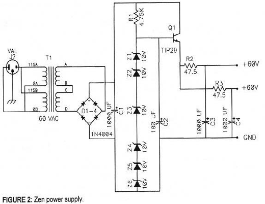
Figure 2 shows the schematic for a power supply with adequate capacity for two channels. The transformer voltage required to produce the regulated 60 volts will be about 50 volts AC. I used an Avel-Lindberg D4007, which is 60 volts with secondaries in series, producing about 86 volts DC across power supply C1. A stack of Zener diodes is used to produce a 64 volt reference biased by R1 and filtered by C2. This stack drives follower Q1.
Additional passive RC filtering is provided. This filtering, along with the filtering provided on each channel, is essential, because the regulation provided by the zener diodes and Q1 has good DC stability but still carries quite a bit of AC noise. As supply noise will appear at the output, we want the power supply noise to be greater than -100 dB below 1 volt, or less than 10 microvolts.
The Parts
In a simple circuit, there are no small roles, only small parts. With the exception of R104 and R204, I have used RN55D type metal film resistors. You are welcome to use anything you choose.
The capacitors in the signal path are metallized polyester film types. “Better” capacitors can be had; maybe they sound better, maybe they don’t. As with the resistors, you may do as your please.
The choice of MOSFETS is slightly more restricted. The devices should be capable of withstanding 50 volts minimum, and 100 volts is preferred. They will need to dissipate approximately 1 watt, and should be equipped with the appropriate heat sink for this.
The IRF510, 520, 610, and 620 are typical parts that are suitable. Higher voltage types are fine, but offer somewhat less transconductance. Higher current types have more capacitance, and suffer from higher distortion at high frequencies due to nonlinearities in this capacitance. The transistor actually used was the International Rectifier IRF610.
Table 1 displays the parts list for two channels and the power supply.
Table 1 displays the parts list for two channels and the power supply.
C1, 3, 4, 101, 102
1000uF,100V
T1
60V AC Avel-Lindberg D4007
Heatsinks
TO-220 transistors
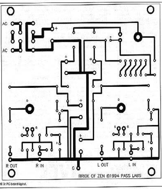
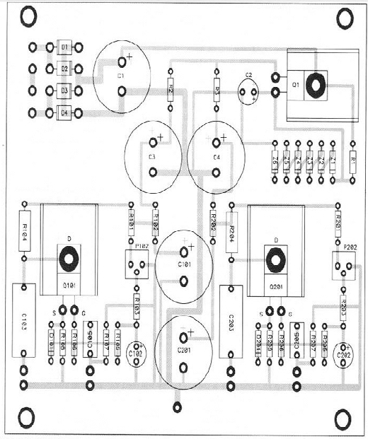
The PC Board
Fig 3 and 4 are the circuit board art and component placement diagram. A simple circuit such as this can easily be constructed on perf board or even with point-to-point wiring, so feel free to do it that way. There is nothing exotic about the layout, and no special requirements to avoid oscillation and such.
Construction Notes
MOSFETs are sensitive to static electricity. Their gate resistance is unbelievably high, but will break down somewhere between 20 and 100 volts, damaging or destroying the transistor. For this reason, I have provided a protection diode in the circuit. Once the circuit is assembled, the transistor will be safe, but until it is, the MOSFET should be handled carefully to avoid exposure to static electricity.
If you can locate a dual volume control potentiometer at 5 KOhms, you will want to use it. Higher values are OK, but result in higher source impedance. If you use short cables between the preamp and a Zen, you should be able to get by with up to 25 KOhms, which will give a maximum source impedance of 6 K ohms. If you can’t find a suitable dual pot, simply use separate level controls for each channel.
The input select system consists of input connectors and a 2 pole rotary switch for a selector. It is preferable to shield the cables between the inputs and the switch, and between the switch wiper and the circuit input. If you want to implement a tape output, you can do so by tapping off the wiper of the selector .
It is useful to put some distance between the transformer and the audio circuitry in order to avoid noise caused by the stray magnetic fields of the transformer and primary and secondary wiring.
I leave the AC power hookup to you. I recommend using an approved commercially available line filter / input receptacle on the AC line, with a .125 amp slow blow fuse.
We will want to ground the chassis to circuit ground, and for safety it is desirable to also earth ground the system through the third conductor of the AC line cord. This occasionally results in ground loop noise, and if it does, I recommend grounding the system to earth through a 10 ohm 5 watt resistor as an alternative to simply floating the chassis. If there is any question about safety in AC power wiring, it is important to consult a qualified technician.
Objective Performance
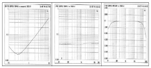
Fig 5 shows the distortion characteristic of the circuit from .1 to 10 volts output. The distortion is fairly pure second harmonic, generally regarded as the least offensive variety. The distortion curve is monotonic, that is to say, it increases smoothly as the voltage increases, and its first derivative is positive. At the bottom of the curve we begin to see some noise, which is the increase in the curve below .3 volts.
Fig 6 shows the distortion versus frequency of the circuit at 1 volt output. It is flat.
Fig 7 shows the frequency response of the circuit. The bottom end rolloff reflects the output and input coupling capacitors. To extend performance to lower frequencies, use larger capacitors. At the high end, the circuit is down 1.5 dB at 200 KHz, and part of this is the test setup. The high frequency rolloff is a function of the capacitance of the MOSFET.
Subjective Performance / Conclusion
It is in this spot that the author elucidates the sonic astonishment which awaits the amateur upon completion of the project. I will not disappoint you. It sounds marvelous. Really. No Kidding.
Even if you didn’t build the Zen amplifier, you owe it to yourself to do this one. Stay tuned for Part 3, The Son of Zen.
White papers and literature still available from Pass Labs, PO BOX 219, Foresthill, CA 95631. tel (530) 367 3690 fax (530) 367 2193
Copyright 1994 Nelson Pass