Zen Variations 3
Nelson Pass
Introduction
In Part 2 we developed a new active current source for the Zen amplifier. In this part, we create a power supply regulator suitable for the Zen amplifier projects.
Previous versions of the Zen amplifiers had no power supply regulation at all, or used capacitor/inductor/capacitor "pi" filters to smooth the ripple on the DC supply lines. In keeping with our philosophy of simple-aspossible, we want to develop a supply regulation system which gives us good regulation, with low AC noise and a stable DC value.
The need for a good regulator is obvious enough. As simple as they are, the Zen amplifiers do not have particularly great power supply rejection ratios (PSRR), the measure of how much of the power supply variations bleeds into the signal path. In the original Zen amplifier, ripple voltages of 1 volt or so typically caused 2 milliVolts or more of the same noise on the output of the amplifier. In this case the PSRR is about 500 to 1, or about -54 dB. 2 milliVolts might seem sufficiently low, that is until you hook the amp up to a 110 dB sensitive horn midrange, and then you will start looking for less noise.
You can make the PSRR of the amplifier higher, or you can clean up the supply. A "pi" filter will take out most of the ripple, but will not stabilize the value of the DC against fluctuations in AC line voltage. For this you need an active regulator.
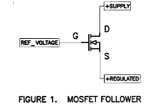
A Basic Regulator
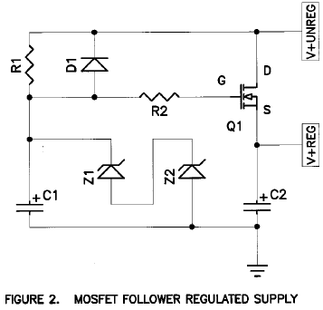
Figure 1 shows an N channel MOSFET set up as a voltage follower regulator. The Drain gets power from the positive unregulated supply, the Gate is presented with a positive reference voltage, and the Source delivers the value of the reference voltage minus the Gate-Source voltage of the MOSFET (Vgs), which is about 4 Volts. To get the correct regulated output voltage, the reference will be adjusted by this amount greater than the desired output.
The output impedance of this circuit is fairly low, being the inverse of the transconductance figure of the MOSFET, which for the IRFP240 is about 5 Siemens, which means that the output impedance will be about .2 ohms.
more Volts more of unregulated supply voltage than the output voltage. 4 of those Volts are used up by the Vgs of the MOSFET, and about 3 Volts are required send 2 mA of current through R1 at 1500 ohms.
If the capacitance of C1 is substantial, we will want to include D1. D1 provides a path for the charge on C1 in the event that the main or regulated supply is discharged much more rapidly than C1, in which case the voltage on C1 might be enough to damage the Gate of the MOSFET Q1, which is rated at a maximum of 20 Volts Gate-Source. A high value of C1 not only improves the value of the noise on the regulated supply, but also gives a very slow turn-on time, which can aid in avoiding transient turn-on noises in the amplifier, depending on the design of the amplifier. In the case of the Zen circuits, it is a definite help.
R2 is included to suppress any parasitic oscillation on the part of the MOSFET. The intrinsic bandwidth of a MOSFET is very high, and this much speed in a part can make an oscillator out of even the modest stray capacitance and inductance found in ordinary hook up wire, so we slow it down just a bit with a Gate resistor.
C2 is just some more capacitance to ground. It helps to stabilize the high frequency response, and like C1, can be large or small, according to taste and need. Large values of C2 will lower the output impedance of the regulator circuit, as the output impedance becomes .2 ohms in parallel with the impedance of C2 at any given frequency. To substantially lower the impedance at low frequencies takes some
You will note that R1 has been increased to 1500 ohms for the purposes of the next section's modification.
Q5 in this circuit must dissipate the amplifier's bias current of 2 Amps with 10 Volts across the Drain to Source. This equals 20 watts of dissipation, and Q5 should have the appropriate heat sinking for this, which would be approximately 1 deg C. per watt.
(In Part 2 of the Zen Variations, resistor values were given as "three digit and multiplier", which meant that 1000 in the schematic was a 100 ohm resistor, and that is how my RN55D resistors are marked, as well as the banding convention used in other 1% tolerance resistors. However this has created so much confusion and complaint in the readership that I will hereafter use the older convention in an effort to end the ongoing flood of email.)
The performance of the circuit of Fig 3 is quite good, taking the Zen amp to 20 watts at .7% distortion. The unregulated supply for this circuit had an AC ripple of 3 Volts peak-to-peak, and regulated supply's noise was 10 mV peak-to-peak, which is a reduction of 50 dB. It resulted in a few microVolts of supply ripple on the output of the amplifier.
The output voltage of the regulator varies with the output current of the amplifier, and with 1.8 amp output peak, we saw a .35 volt peak on the output of the regulator, giving a .2 ohm output impedance, close to what we expected. If this is not good enough, there are still ways to improve it without recourse to feedback.
appreciates a quiet and stable supply, and previously we have only seen it with "pi" filtering.
We do not modulate this particular supply as it sources two halves of a balanced channel which operated out of phase. The supply draw of this circuit is truly constant at all times, a "zero sum game" for the circuit. By contrast, the Zen has a constant draw averaged over time, and the instantaneous draw from the supply reflects the output current of the amplifier.
Paralleling Devices for More Current
There are instances where we want the supply to deliver more voltage and current. Since the MOSFETs and other parts can easily be set up to handle 100 Volts or more, the issue comes down to current and dissipation. The circuits presented here are capable of 4 Amps continuously with moderate dissipation on the series pass transistors, but more current will require parallel devices.
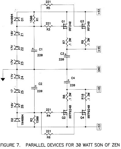
Figure 7 shows additional parallel transistors added to the circuit of figure 6. These devices are best matched for Vgs within .1 Volts to ensure that they do a good job of sharing the output current. They also use Source resistors at .1 ohm each to further encourage the transistors to share the current equally.
You can parallel as many matched MOSFETs in this manner as you like, each with it's own Gate resistor, and stability will not be an issue. The output impedance of each transistor will be the Source resistance plus the inverse of the transconductance of the MOSFET, which in this case
In Conclusion…
So now we have a nice simple regulator for this and future Zen amp projects. It is not the highest performing regulator, but we don't need high precision for these amplifiers, and as long as the amplifier is biased Class A, any voltage appearing on the supply will be a linear function of the output waveform, and is benign in its character. Of course if you want a lower source impedance, you can start paralleling devices and/or piling on the output capacitance.
In Part 4 we will wrap up the Penultimate Zen with an input buffer and PC artwork.
This figure is not particularly great as a regulator, and ordinarily we would look to improve on it, usually by enclosing the regulator transistor in a feedback loop to correct for this variation. If this were a higher power Class B or AB type amplifier, such an output impedance could easily result in one or two Volts of nonlinear distortion signal in the power supply, and this would bleed into the output circuit as distortion.
With a Class A amplifier, we have the advantage that the current draw from the supply is a linear function of the output current, and so no distorted "half waveform" is seen impressed on the supply voltage. This being the case, the importance of the output impedance becomes less, and we can consider using this follower without feedback.
Figure 2 embellishes on the concept of the one transistor follower. In this circuit R1 is used to bias up the Zener (not related to Zen) diodes which provide the reference voltage. A capacitor C1 is placed in parallel with Z1 and Z2 to remove the intrinsic noise of the Zeners and further smooth the ripple out of the reference voltage. C1 is not essential, and can be a large or small value.
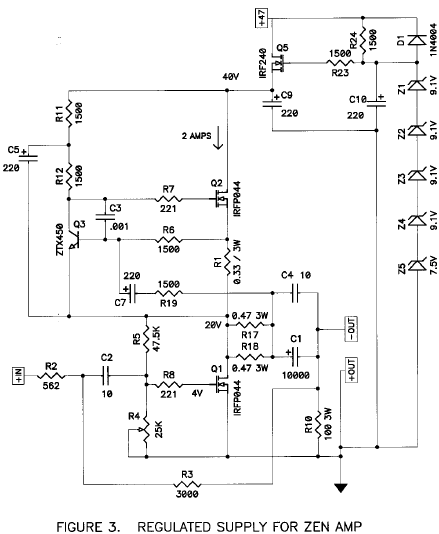
We will want to send about 2 milliAmps or so through the Zener diodes to get it into the proper voltage region. Z1 plus Z2 have been chosen to be 4 Volts above the desired regulated voltage, and some more voltage will be needed across R1 to deliver the current through Z1 and Z2. If the regulated voltage is to be 40 Volts DC, and the Zener diodes sum to 44 Volts, and the unregulated supply is 47 Volts, then R1 will have 3 Volts across it, and will want to be about 1500 ohms in value.
As a practical matter, this is a lossy circuit, in that it takes some 7 or
serious capacitance, for example 40,000 uF represents .2 ohms at 20 Hz.
The circuit does not actually require the use of Zener diodes to work well for many purposes. If you take the Zener diodes out, then the circuit simply filters out the AC voltage from the supply value, leaving the DC value and giving a DC output voltage about 4 Volts less than the unregulated voltage. I prefer the value stability with the Zeners in, as they represent only a small investment in parts.
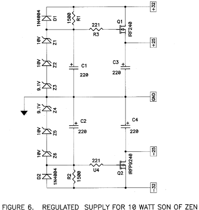
In this project I use several Zener diodes in series, building up higher voltages from smaller voltage Zeners. I do this mostly for reliability. Five 1/2 watt Zener diodes at 9.1 Volts each can take five times the bias current of a single 45.5 volt Zener, and if the AC line voltage goes very high, it might have to. Using multiple Zeners in a stack also gives some flexibility in getting exactly the value you want, as seen in Figure 3, where one of the 9.1 Volt Zeners is replaced by 7.5 Volts to get the 44 Volts desired. You might ask me, "Why do you always use 9.1 Volt 1N4739's in your projects?" The answer is that I have a lot of them on the shelf, and I am very comfortable with them. You might also ask, "Why an IRFP240 instead of some other MOSFET or even a Bipolar transistor?" Same answer.
A Regulator For Penultimate Zen
Figure 3 shows the circuit of Figure 2 applied to our Zen amp. Q5 is the new name of our pass transistor and Z1 through Z5 form the Zener reference. In this circuit, the unregulated voltage is about 47 Volts, and the regulated voltage is about 40 Volts. R24 passes about 2 mA through the Zener stack, and C9 and C10 provide additional filtering.
The values of C9 and C10 are arbitrary, and can be made quite large or small as you like. As you increase the value of C10, keep in mind that very large caps have some leakage current which might exceed the bias current value, so figure on having less than 10,000 uF or so for C10. Very high values for C9 might have the effect of overheating the MOSFET on turn-on, but by high I mean maybe 100,000 uF. You can eliminate C10 altogether, but I suggest a minimum of .1 uF for C9.
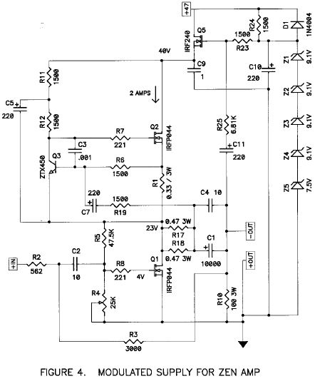
Modulating the Regulated Supply
The 14 watt loss on the MOSFET pass transistor is a bit much to put up with. Figure 4 shows a technique by which we can modulate the regulated supply voltage with the output signal of the amplifier, allowing the regulated supply to swing up to within a Volt of the unregulated supply, increasing the peak-to-peak output swing by about 6 Volts, and our power from 20 watts to 25 watts.
R25 and C11 have been added, communicating a portion of the output voltage of the amp to the Gate of the pass transistor, causing the regulated output to reflect a small version of the output wave and giving the circuit a small boost at high output levels. Note that the output capacitor C9 in this case is now 1 uF so that the regulator does not have to drive a large capacitor. Note also that the standing DC value for the output voltage of the amplifier is not 20 Volts, or ½ the regulated supply, but 23 Volts, to better take advantage of the higher peak supply voltage.
The performance of the Zen amp with this modification is shown in Figure 5, where the clipping point is modestly improved to 25 watts rms.
A Bipolar Version for Son of Zen
We can also build this supply as bipolar. No, not with bipolar transistors, but a supply with both plus and minus voltages for those amplifiers preferring two rails. Figure 6 shows such a version of this MOSFET follower supply applied to a 10 watt version of the Son of Zen. The Son of Zen has a poor PSRR by itself, and relies on the matching of its balanced halves for low noise. It much
is .1 ohm plus .2 ohms = .3 ohms. If you parallel two such devices, you will get .15 ohms, and with 6 such devices you will get about .05 ohms and so on.
Matching MOSFET Redux
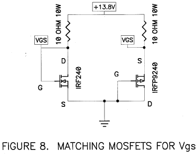
First presented in the A75 project in issue 2/92 of The Audio Amateur, the setup and procedure for matching the Vgs of power MOSFETs is simplicity itself. We repeat it here with slight modification in Figure 8. Using a car battery voltage or a 15 Volt regulated supply, we bias the MOSFET up as shown through a 10 ohm 10 watt resistor, with the Gate attached to the Drain. With the Vgs measuring about 4 Volts, we will see about 10 Volts across the resistor, and about 1 Amp of current through the device. With the devices at about the same temperature, measure the Vgs for a few seconds only (the device will heat up within 20 seconds or so) with a DC voltmeter and make note of the value. Those devices which are within .1 Volts or better can be considered a match for these purposes. The circuit for the N channel devices is shown on the left, and for the P channel devices on the right.
As a practical matter, in deciding how many to parallel, consider that the output devices will be very reliable at up to about 25 watts if provided with enough heat sinking to keep the case at 60 degrees Centigrade or so. To give you a rough sense of where the parts become unreliable, experience shows that when you run them at 50 watts at 70 degrees, you will occasionally lose one, as I did last week. No matter, DIYers are a fearless breed, we keep lots of spares, and it took about 10 minutes to pop another one in.
You can pretty easily substitute NPN and PNP Bipolar Darlington devices as the series-pass transistors in these schematics without loss of quality, and in the case of paralleling devices as in Figure 7, you can do so without matching the devices. Darlington types are necessary, however, for while the current gain of a MOSFET is practically infinite, the Bipolar device requires a finite DC input current. This is typically about 300 or 400 micro-Amps per output Amp. In high current regulators, you will want to provide slightly extra current going through the Zener stack to accommodate this.