A75 Part 2
Norman Thagard & Nelson Pass
Introduction
THE STORY BEHIND the A75 power amplifier continues. In Part I, we discussed its origins and direct predecessor, the Pass A40, as well as some general guidelines to follow before initiating such a project. We covered such topics as MOSFETs and differential pairs. In this concluding part, we will analyze the amplifier's component parts in depth, beginning with the source.
The Power Supply
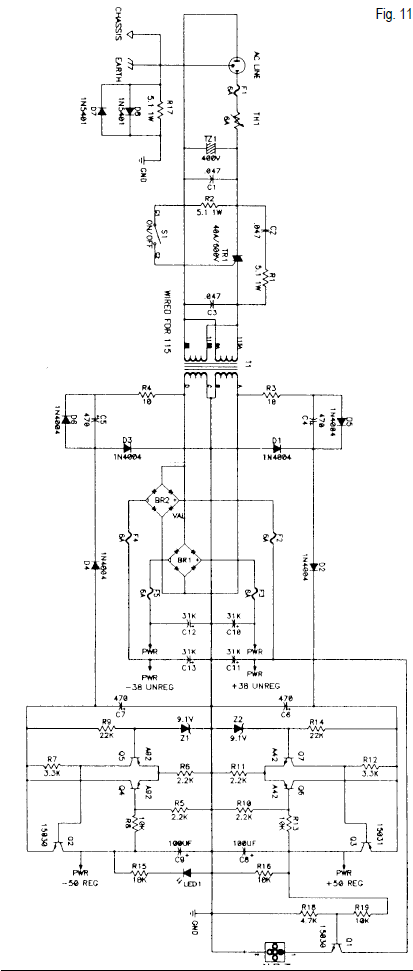
Figure 11 shows the amplifier's power supply circuitry. AC line power enters through the power cord and passes through fuse F1. To reduce the effects of inrush current, thermistor TH1 is employed. At room temperature, this will have a resistance of several ohms, which will limit the initial power supply capacitor charging current. A short while after start-up, the thermistor receives heat from the current passing through it and has a low impedance.
Following the thermistor, we see spike absorber TZ1 which conducts at high spike voltages and which, in this application, protects the triac. In parallel with it is C1, which aids in spike suppression and RF filtering. Triac TR1 is the main power switch. Rated at 40A and 600V, it is capable of withstanding high inrush surges. You can easily trigger it with small switch S1, which is in series with limiting resistor R2. Across the triac is an RC network formed by R1 and C2, which damps out transients across the triac. C3 follows the triac and supplies more suppression and filtration.
The transformer is a 500W toroid with dual 115V primary and 30V AC secondary coils. Figures 11 and fig. 16 show the hookup of the primary coils for both 115V and 230V operation.
The secondary system is comprised of a standard unregulated plus and minus 37V DC supply and a higher voltage regulated supply. The high power unregulated supply drives the output devices of both channels and consists of BR1, BR2, and four large capacitors, C10-13. Two bridges are employed to reduce the work load, and to afford some isolation between the two power supply channels. These supplies will communicate with each other only during the charge pulse which occurs at the peaks of the AC line waveform.
The regulated high voltage supply will drive the front ends of the amplifier channels, and delivers a regulated +/50V at about 150mA. It consists of C4-7 and D1-4, and is formed by a voltage doubler circuit. Without a load, this circuit will double the supply voltage of +/- 35V of the unregulated supply, but without much current capacity. Resistors R3 and R4 slow the charge cycle and reduce the output voltage, which lowers the heat dissipation in the regulator circuits.
Voltage Doubler
Voltage doubler operation is not easily explained, and sometimes you just have to look at it for a while. Since the two halves are independent,
let's look at only the positive half. When transformer tap A swings negative, it will cause C4 to pick up a charge of equal voltage as conducted through D1 from ground. Since tap A will hit about - 38V relative to ground, the capacitor will be charged to approximately 36V.
When tap A swings positive, the voltage on the capacitor will swing with it, plus the 36V at which it has been charged. When tap A reaches +37V, the voltage on the capacitor's positive side will now be at 37V + 36V = 73V. This 73V will conduct through diode D2 and charge capacitor C6 up to about 72V. The result of both the positive and negative voltage doubler circuits is + 72V and - 72V, but is poorly regulated with large ripple voltage.
The remaining circuitry consists mostly of the plus and minus regulators for the high voltage front end supply. On the positive side, R14 sends current through Z2 to create a 9.1V source. This biases up the differential pair formed by Q7 and Q6 through R11. With an input voltage at 9.1, the voltage across R11 will be about 8.4V or 4mA.
Q7's collector output drives the base of Q3, forming another example of our friend, the op amp. Q3's output is fed back to the base of Q6 (the op amp minus input) through resistor network R10 and R13. These form a voltage gain of 5.55, which multiplied by the input voltage of 9.1 gives an output voltage of 50.5V. Capacitor C8 provides some filtering and assures the loop stability of our op amp when used as a power supply regulator. Note that R11 is held at a constant voltage by the constant voltage input, eliminating the need for a constant current source to improve the performance.
Cooling for the output stage heatsinks is provided by a DC fan. You can control its speed very easily by varying the DC voltage. Generally, running these fans at full voltage will create much more noise than the audiophile will wish to hear. Our fan will be run slightly under 15V (although it is rated at 24V), which will be enough to reliably push air through the heatsinks but will not be too noisy.
The fan voltage is derived by running the positive regulated 50V supply through resistive dividing network R19 and R18. This reduced voltage is
their fairly low capacitance and greater linearity at lower currents compared with higher current types.
Q3, Q9 and Q7 (and their complements Q6, Q10 and Q8) operate at higher currents. Q9 and Q10 also operate at significantly higher wattage, and a larger transistor was appropriate. We chose IRF510 and its complement IRF9510. The output devices were chosen with similar criteria. The high-performance IRF230 costs as little as $2 each in quantities.
For all these devices, there is some latitude in alternate parts. When you call the distributor, it is unlikely he will have all of them in stock (although one of the reasons you see them here is that they were available when the amp was designed). Here is a list of alternatives from International Rectifier.
IRFD110: N-channel, 1W, O.5A, RDS < 1ohm
Examples: IRFD113, IRFD123, IRFD120, IRFD223, IRFD210, IRFD220
IRFD9110: P-channel, 1W, 0.5A, RDS < 1ohm
Examples: IRFD9113, IRFD9123, IRFD9120, IRFD9220
IRF510: N-channel, 20W, 4A, RDS < 1ohm
Examples: IRF512, IRF612, IRF610, IRF710, IRF712
IRF9510: P-channel, 20W, 4A, RDS < 1ohm
Examples:IRF9512, IRF9612, IRF9610
IRF230: N-channel, 75W, 9A, RDS < 1ohm
Examples: IRF130, 2N6756, IRF231, IRF232, IRF233, IRF230, N6758, IRF330
IRF9231: P-channel, 75W, 9A, RDS < 1ohm
Examples: IRF9230, IRF9232, IRF9233, IRF9130, IRF9132
Any of these devices would serve as equivalent replacements. They
Consistency is the most important thing here. The given voltage is 15 and, adjusting for about a 4V VGS, we will see about 11V across the resistor.
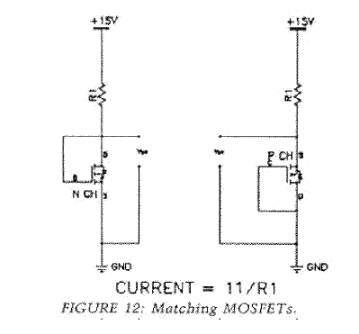
We are looking for as much matching of the input MOSFETs as possible at a current of 5mA. For this test, we use an R1 value of 2.2kohm. Measure the voltage between the gate and the source. Write it down on a piece of masking tape or a sticky label and place it on the part. Keep in mind the caveats about electrostatic discharge: touch ground before you touch the parts.
Matching input MOSFETs is critical, because they must share equally the 10mA of bias current from the current source, and they will not do that unless their VGS is matched. At 5mA current, they have an equivalent source resistance of about 15ohm. Assuming we want them to share the current to within 2mA, we calculate the required VGS match as follows. Using the formula V = IR, we see V = 0.002 x 15, which gives us 30mV. The VGS of the input devices should be matched to within 30mV at 5mA current. The matching is only essential within a given pair; you do not have to match the Ps to the Ns, or match to devices in another channel.
If you are unable to find input devices matched to within 30mV, you must insert resistance in the source to make up the difference. The resistance is calculated by the difference of the two values of VGS divided by 5mA. For example, if the difference in VP1GS is 100mV, then 0.1/0.005 = 20ohm. You would then place 20ohm in series with the MOSFET source having the lower VGS.
We use the same test setup for the MOSFETs in the TO-220 packages but at a higher current (20mA), so we use a 560ohm resistor. No matching is required for these devices; we are just checking to see that the VGS is between 4-4.6V and that they work.
We will measure the output device VGS at about 170mA. You can achieve this with either a 56ohm at 2W resistor, or two 100ohm at 1W resistors in parallel. We are looking to obtain a reasonable match within a parallel output bank of each polarity of each channel, so we want two groups of 12 with matched N- channel devices, and two groups of matched P-channel devices.
The VGS voltages of our test samples gave the following spread:
------------N-channel ---- P-channel
Min. VGS ---- 4.00V ------ 3.79V
Max. VGS --- 4.57V ------ 4.15V
Avg. VGS ----4.42V ------ 4.01V
We also measured the transconductance by taking another reading for each device at a higher current (0.5A), just to see what kind of variation we got. The transconductances measured from a low of 1.19 to a high of 1.56, with the average at about 1.35. Within this amplifier's general operating curve, each output will vary its current by about 1.3A for every volt of its VGS change. For 12 devices in parallel, we expect about 15A for each such volt.
By placing 1ohm source resistors on each transistor, we can assure
hundred of you will write to ask how to bias for Class A into 1ohm.
Let's review a couple of things. The peak voltage on a clean output sine wave is 1.414 times the average voltage, and the peak wattage is twice the average. An amplifier that delivers 75W into 8ohm average will need to deliver a peak of 150W, which requires a peak voltage of 34.6: V = SQRT(150X8).
This 34.6V peak will mean that, allowing for 2V loss, you need a supply voltage on the output stage of at least 37V. A transformer having split 28V secondaries will generate this. These secondaries will peak at 28 x 1.414 = 40V, with at least 1V lost to diodes and ripple on the capacitors. The transformer secondary voltage will vary with load; the specified transformer will load down to about 37V DC when bias is applied.
The peak current from that 34.6V means peak amperage into 8ohm of 33.5/8 = 4.3A. On a push/pull Class A amplifier, the peak output current in Class A mode is equal to twice the idle current, which will be 2.2A. Into lower impedances, it will be higher.
Now 2.2A through a bank of transistors having 37V across it comes out to V x A = 2.2 x 37 = 81W on the positive bank. You will have another 81W across the negative bank, for a total idling dissipation of 162W. Again, this will be slightly more than twice the rated 8ohm power. If you want to run the amplifier at 150W Class A into 4ohm, you can do it, but you will be idling at 4.4A or 324W. You would need a larger transformer.
By the way, the transformer is selected very simply: it should have the appropriate secondary voltage at twice the VA rating of what you will use. Maybe a little less if there is a fan playing air across it. For this amplifier, we will be running about 330W and using a 550W transformer and a fan.
Anyway, here we are with 330W to dissipate in our heatsinks, and we have made it a rule of thumb not to exceed 55°C on a heatsink. Human skin has the remarkable characteristic that we think 40° is comfortable, 45° is hot, 50° is very hot, and 55° is untouchable. This expanded
Pass recommends the book Zen and the Art of Motorcycle Maintenance, by Robert Pirsig.
PC Boards
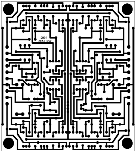
We will not go into PC board construction here, but are presenting artwork and making disk files of Gerber artwork available for those of you who want to use a PC fabrication house. These shops once accepted paper or taped layout artwork and would create the appropriate film pattern. Now it seems that they all require Gerber files exclusively.
The artwork presented here is for the front end and power supply boards. The output stage board is not shown on the presumption that you will probably end up with a slightly different heatsink layout. However, the pattern is included with the Gerber files, if you want it. An
fed to the base of emitter follower transistor Q1 whose collector is attached to the positive unregulated supply (so as not to load the regulated supply, and for lower dissipation), and whose emitter drives the fan's positive lead. The negative lead goes to ground. Be prepared to adjust the values of R19 and R18 to get the fan speed you want. You may be tempted to run it very slowly for low noise, but be certain that it always starts rotating on turn-on. Of course, you may decide to simply use very large heatsinks and dispense with the fan.
TABLE 1
Power Supply Parts List
Part List for Power Supply Board
C1-3
0.047, line voltage, Digi-Key #P4604
C4-7
470, 100V,electrolytic, Digi-Key #P6522
C8,9
100uF, 63V, electrolytic, Digi-Key #P6735
C10-13
31000, 50V, computer grade
Fan
DC fan, 24V, Digi-Key #P9996
TH1
Thermistor, 6A, Digi-Key #Q6040J7
TZ1
TZ, 400V, Digi-Key #P7092
T1
Transformer line, 550VA 60V CT, Avel
Transformers inc., D4060
Component Selection
You will find resistor and capacitor specifications in Table 1, along with some Digi-Key part numbers. Use as high quality parts as you like, but when considering substitutes be aware of how well they will fit on the PC board.
Gain device selection presents a narrower range of alternatives. We have chosen to use International Rectifier MOSFETs exclusively, because of their consistently high quality, moderate cost and lead time, and US manufacture.
For the input devices, we chose the IRFD110 and IRFD9110. They worked better than anything else from the catalog, mostly because of
have the same wattage ratings, more than adequate voltage ratings, and similar trans-conductance figures, but they will have different costs and availability. Other devices not mentioned here will also work well, as long as they have similar characteristics. Some of them are secondsourced by Motorola, and you can also consider devices from Toshiba and Hitachi. It will be helpful, but not essential, if they offer the same cases and pinouts. We have deliberately chosen the output transistors in TO-3 packages, but there is a large equivalent selection in plastic packages. You should not be afraid to use them. Because of the audio circuit's simplicity, its design is very forgiving of substitutions. The primary criteria are adequate voltage, current, and dissipation ratings.
When making substitutions, you should get one type or another. Mixing different devices together will not make matching easier. For that matter, it is generally helpful if they have the same lot codes, which means that they were made together and will tend to have similar characteristics.
We recommend buying more devices than you think you'll need. Even if you don't experience failures, you may find during testing that some are sufficiently different so that you don't want to use them. Having a sizable population is a real help if you are planning on selecting and matching.
Component Testing
After you acquire the devices, you will need to test them. You might consider running lots of tests on these transistors, but only one is essential: measuring gate-source voltage versus current. The greatest variations occur here, and it is necessary to do some matching to get proper performance. This test will also tell you whether or not the device is broken.
The test is simple and requires a power supply, a resistor, and a DC voltmeter. Figure 12 shows the test hookup for N- and P-channel types. The supply source resistance (R1) is nominal, and is found from
adequate current sharing for a fairly wide range of VGS. In Class A bias, we will be operating at about 200mA/device, which will place 0.2V across each source resistor. A variation in VGS will cause the bias to be unequally distributed between the devices. For example, for a 4.6V device in parallel with a 4.5V device, the first will run at about 160mA at 6W and the second at about 240mA at 9W.
Remember that each of these devices is rated at 75W on a cold heatsink, and maybe 50W on a hot sink. We are only going to bias them to about 8W each, so they're not going to break from a little unequal distribution. Nevertheless, we like to see the load shared, and recommend that you group the outputs by VGS as closely as possible. Matching within 0.2V will work, and O.1V is even better. Within a population of 150 transistors, you can easily get 12 sets matched to O.1V VGS at 200mA.
Heatsinking
Heatsinks are "first-and-foremost" things. We will start by figuring out how much we really need. A 75W pure Class A push/pull amplifier will theoretically operate at 150W of idling dissipation, 170W when all is said and done. You can put more wattage into 8ohm by cranking up the supply if you pay close attention to your heatsink requirements. You will also need to consider this if you want to maintain Class A bias down to a lower impedance level. The amplifier will operate very cleanly into low impedances anyway, so this is not essential. But we know that about a
temperature sensitivity has a lot to do with injury prevention, and is also very convenient for judging whether or not heatsinking is adequate. If you can't touch it, it's too hot.
Given a 50°C heatsink in a 25° ambient temperature, the difference is 25°. We want to build a heatsink system which will only rise 25° while dissipating 330W. This gives us a thermal resistance figure of 0.08 °C/W. Look in the heatsink catalog and find one with 0.08°/W rating. (Now you know why there are so few pure Class A power amplifiers on the market).
Maybe we can use several smaller sinks, say 12 with 1 deg/W ratings. In the Thermalloy catalog you can check out #15217, which Pass designed to use in Threshold amplifiers. In 6" lengths it is about 0.6°/W, and you would only need eight of them. When you think about the number of amplifiers on the market claiming pure Class A at hundreds of watts, and compare their heatsinking to this, you might conclude that something funny is going on (and you would be right).
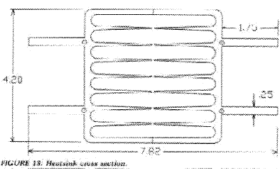
We chose to use four pairs of forced air sinks at 5" lengths whose cross sectional dimensions are given in Fig. 13. The surface area is about 54 in²/ inch, and it is very similar to the Aham Tor #3750 or the discontinued #6180.
This sink's rating is 1.5°/section/3", so for 5" it will be about 0.9°/W. For eight sections {four pairs), we are down to 0.1125°/W. We will run enough air through them to double their efficiency, for about 0.06°C/W of thermal resistance, which should be enough. If it isn't, we'll turn up the fan.
Under these circumstances, the output devices will be sitting on sinks at about 50° and, with dissipating 8W apiece, the case temperature will be up another 10° or so. With a case temperature of 60°, the data book on these 75W devices tells us they are rated at 55W. We will be using them at about 15% of rated capacity. This means two things: they will last a while, and you will be able to kick 70A into that 0.3ohm electrostatic load, at least on peaks.
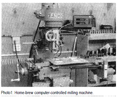
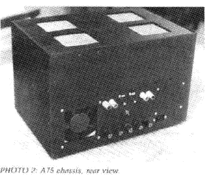
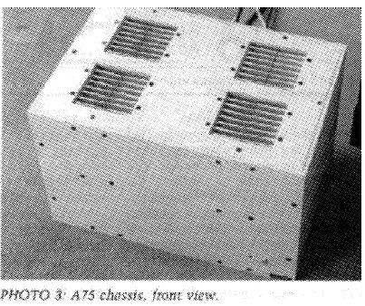
The Chassis
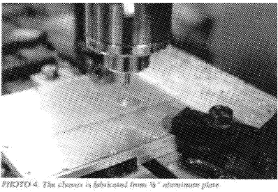
Many people think building a chassis is the hardest part. Pass solved the problem by first building a machine shop, with five computer-controlled milling machines (Photo 1). That's how we got this chassis, which was carved out of aluminum slabs (Photos 2, 3, 4).
Most of you will show a lot of creativity in this area. Buying a prefab chassis is a good idea, but unless you have some experience drilling sheet metal, it will still not be easy. We suggest you check out some available hole punches. You put them in a small hole you have drilled and then crank on the bolt. They work adequately and are well worth the expense.
Maybe you should consider making friends with metal shop workers (they like big amplifiers, too), or enroll in night school machine shop. Whatever you do, keep in mind that the chassis will be the temple in which your project is housed, and do a good job. Plan it carefully, take your time, and try not to be too cheap about it. For proper perspective,
output stage board is a good idea for this project, because the MOSFET gate and source resistors are best located at the output devices, and a PC board is most convenient for holding them.
Power Supply Assembly
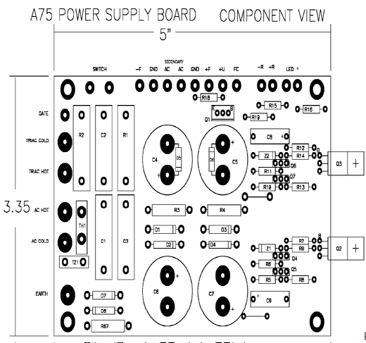
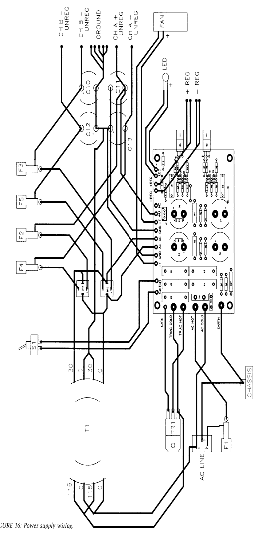
You've got a chassis and PC boards, and you've tested and matched the MOSFETs. Now you will need a power supply to test the front end, so let's build it first. Table 1 is the power supply parts list. Figures 14a and 14b are the PC board power supply and the component placement. Figure 16 shows it wired up in the amplifier. Not much to note here except that the artwork shows component side, not copper. Diodes D5 and D6 are tacked on the back across the terminals of C4 and C5, because they were added after a hundred boards were made. Note that transistors Q2 and Q3 will be operating at about 1.3W each, so give them adequate heatsinking.
You can mount them to the chassis beneath the PC board if you wish (taking care to insulate the tab from the chassis), or you can mount them
vertically with a heatsink such as a Thermalloy #6106. The TO-220 transistor Q1 for the fan control will want some sinking. We used the 6106 for that, also. Although not essential, it will not hurt to put some sinking on the TO-92 transistors Q4-Q7, in the form of little press-on tab sinks.
In wiring the power supply (Photo 5), take special care with the AC power line circuitry (Fig. 16). Vital for safety is a well attached earth ground connection. The middle (earth) pin on the AC line input connector must be attached directly to the chassis with at least 18- gauge wire. Take care to establish good mechanical attachment of wiring to connector lugs before soldering, and maintain adequate
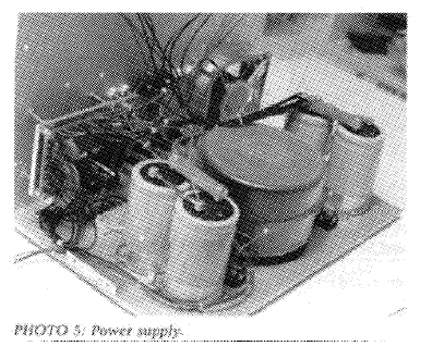
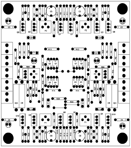
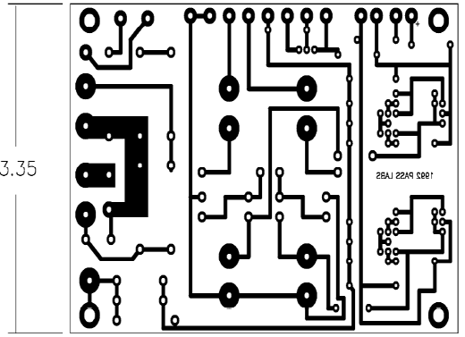
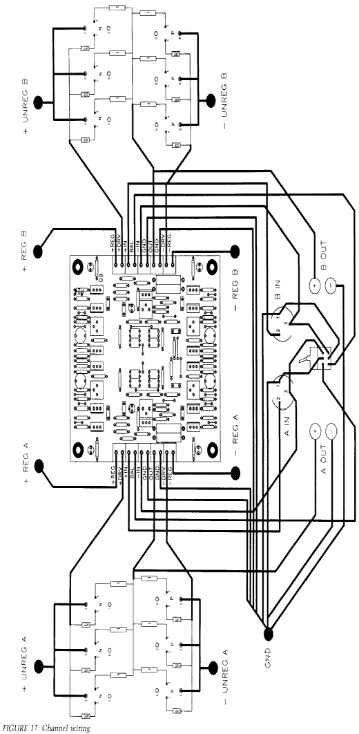
the high current flows, and the shortest, most direct path is desirable. The connection of the gates to the front end board is less critical. When assembling the output stage, remember Mr. Static Discharge. Until the amplifier is completely assembled, touch ground first. Table 2 is the front end parts list for one channel only, so double it for two channels. Figure 15a is the PC artwork for the front end board; Fig. 15b is the component placement. In Figs. 15a and 15b note that again both views are from component side, not copper. The board carries both left and right channels, which are virtually mirror images of each other. You will find that each part number occurs twice, once for each channel. The TO-220 transistors Q9 and Q10 will require heatsinks, since they operate at slightly less than 1W. Q7 and Q8 could use a heatsink, too, and the Thermalloy #6106 will fit here if you carefully watch your clearance. Figure 17 shows the integration of the front end, output stage, and power supply. To make life a little easier, we have specified a screwdriver-operated terminal bus on the front end connections and on the secondary connections of the power supply (Digi-Key part #ED1609). This allows separate testing of the front end and helps when repairing or modifying the amplifier. The connectors are rated at 16A, but they will see very little current in this use and will not cause any degradation in performance. Don't wire up the amp yet; we will be testing individual subassemblies first.
Power Supply Testing
We will first test the power supply with the front end and output stages unattached. Use a Variac for the AC line source so you can take the voltage up slowly, looking for faults. If you don't have a Variac, at least wear safety glasses; rubber gloves are also recommended. In addition to a Variac, you will need a voltmeter.
We recommend that you place resistors across the power supply capacitors during testing to slowly bleed off the charge after the AC power has been removed. You don't want a fully charged capacitor when you solder up the rest of the circuit. C10-13 should each have a bleed resistor across their terminals. The resistor value should be chosen so it does not fail at 40V, which would be 1.6kohm or more for a 1W resistor,
spacing between live connections and other conductive pieces.
The triac used here has a case which is insulated from the circuit, and is mounted on the chassis with a 6-32 screw. Bend the leads upward from the chassis to ensure good clearance between it and the AC live pins. The center pin MT1 is on the input side of the circuit attached to TH1, and the small pin is on the gate attached to S1.
The chassis is hardwired to AC ground, and the secondary power system ground is attached to that through R17 and D7 and D8. This connection provides for safety in the event of failure through the transformer, and helps to reduce ground loops. When the potential voltage from secondary (signal) ground to chassis is low, current is conducted through R17, whose value is just high enough to damp out ground loops caused by magnetic fields. In the event of major current flowing to earth ground, the high current diodes D7 and D8 will conduct and hold the voltage difference to about 0.7V.
Output Stage Assembly
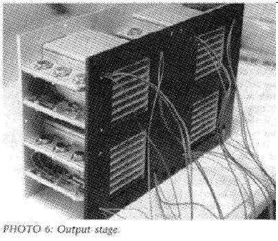
The power transistor output stage (Photo 6) must be isolated from the heatsink electrically, so you must use nylon cylinders in the heatsink mounting holes (to prevent the #6 mounting screws from touching), and mica or silicone insulators for the TO-3 cases. If you use the mica insulators, you must also use thermal grease to ensure good thermal contact. The gate and source resistors are part of the output stage. Some sort of PC board for the output stage is a good idea.
The collector connection wires go straight to the power supply, and the source connections go straight to the output terminals. These are where
Table 2
One Channel Parts List
Capacitors:
C3,4,7
4.7uF, 16V,
electrolytic
C5,6
220uF, 16V,
electrolytic
Resistors:
and 3.3kohm or more for a 1/2W resistor. If you choose, you can make the resistors permanent.
Remember: safety first. Whenever you work inside the amplifier, you should check across the capacitors to make certain they are not carrying voltage. Unless required for a test, the AC line should be unplugged.
To begin testing, place a fuse in the AC line fuse holder, but do not place the secondary fuses. With the power switch in the on position, set your voltmeter to AC at a scale which will read 10V or more. Plug the AC power connector into the Variac and slowly bring up the voltage while reading the AC across thermistor TH1. You are checking to see how much current is being drawn, and you do that by measuring the AC voltage across the 5ohm of the cold thermistor.
The convenient points at which to measure this voltage are the fuse terminal on one side and the triac MT1 (middle) terminal on the other. As you slowly turn up the Variac, the AC voltage across the thermistor should remain low (1V or less). If it is more, you probably have a fault: turn off the Variac immediately. Don't turn the Variac up more than a third of the way if you don't see more than a volt. You are just checking that nothing is shorted.
Now set the voltmeter to read DC volts up to 100, and read the voltage from ground to the regulated supply system outputs. These points are the same as the cases {collectors) of Q2 and Q3 on the supply board. This voltage is designed to regulate at about 50V, and you should see it increase as you slowly turn up the Variac. The two outputs should hit + 50V and - 50V and stop when the Variac is about three quarters of the way up. (By the way, "all the way up" on a Variac is more than 120V, which is represented by a dot on the dial at 85; do not turn the dial past the dot.)
If the regulated output locks in at about 48-53V, you are in good shape. Next test the unregulated voltage from the voltage doublers which supply this power. It should be about 72V, and can be read off the supply side of R9 and R14 on the supply board.
If it is working OK, let the regulators run for a couple of minutes. Then shut off the power and let it bleed down for a few seconds. Disconnect
the power cord, and touch the transistors on the power supply board to see whether any are hot. None of them should be more than warm.
Now test the main supply. Check the polarity of the main capacitors again {this is your last chancel. Place the secondary fuses in their holders, plug the AC cord into the Variac, and slowly bring up the voltage while monitoring the DC across the big capacitors C10-13. Wear safety glasses. When the Variac is all the way up, you should see about 40V DC across each capacitor. Now measure the AC voltage, which should read only a few millivolts. If it reads an appreciable fraction of a volt, something is drawing lots of current (possibly the capacitor itself-- double-plus ungood).
The fan should be running, with the Q1 emitter reading at about 15V. You can adjust the voltage by adjusting the value of R18 on the power supply board. Increasing R18 up from 4.7kohm will speed up the fan. DC fans can be run at considerably lower voltages than their ratings and made to spin quite slowly. As the voltages go down, however, you must be certain the fan will start, which places a practical lower limit on its speed. If you wish for a slow fan speed and are having a problem starting the fan, you might consider placing a capacitor in series with a resistor across R19 for a higher initial voltage. A good value might be 47uF at 50V with the plus terminal pointed toward the positive supply and in series with 10kohm. Place this combination in parallel with R19.
If the voltages check out, disconnect the AC power. Let the capacitors bleed off, and remove the secondary supply fuses in preparation for the next test.
Front End Testing
The front end board is designed to operate without an output stage. This greatly facilitates testing, as we can adjust the front end at length without any chance of damaging the output stage. We can also easily isolate problems. The simple nature of the circuit topology makes problems due to front end and output stage interaction unlikely, which is also convenient. The two front end channels can be tested independently, as their only common connection is signal ground. Remember Mr. Static!
Test the front end circuits one at a time by connecting the plus and minus regulated supplies ( +REG and -REG), and the positive input ( + IN). The BAL connection, the -IN connection, and the GND next to it are tied together and go to ground. The + DRV, - DRV, and the GND next to it are not connected. The +IN connection goes to the source, which should be an oscillator at 1kHz variable from 10mV to 1V. Set the output at about 100mV. The OUT connection goes to the input of an oscilloscope for output waveform viewing.
The potentiometers should be set so the P3s in the board center are at maximum resistance (full counterclockwise), and the P1s and P2s are at the halfway point.
Again using the Variac to slowly bring up the supply, apply power to the front end board. At about halfway up, verify that the DC voltages across the zener diodes Z1 and Z2 are at 9V; then verify that the DC voltages across R9 and R10 are at about 5V. If this is the case, we will know that proper current is being fed to the input differential transistors.
Once you are satisfied with the first channel's operation, disconnect it and perform the same connections and tests on the second channel. When you are done, unplug the AC power.
Testing Finished Channels
Completely wire the amplifier as shown in the diagrams. Watch for static, and ground yourself before touching circuits and wires. Place the secondary fuses F2- 5 in their holders. Using an ohmmeter, verify that Pin 3 of the amplifier input is attached to ground when the balance switch is set to unbalanced mode, and leave it there.
Attach an oscillator at 1kHz at 300mV to both inputs, driving Pin 2 of each channel. With a dual-trace oscilloscope, monitor the outputs of both channels. Use one or more DC voltmeters to monitor the current through each channel's output stage by reading the voltage across one of the 1ohm source resistors R34, and so on. Do not yet attach a load at the output.
Slowly bring up the Variac while monitoring each channel's output, and also the DC voltage across the 1ohm resistors. The output waveform should be about 6V AC with no DC offset; the DC values across the 1ohm resistors should be near zero. Slowly adjust the P3 potentiometers of each channel clockwise and observe the DC voltage across the 1ohm resistor as it increases. Set that value to about 150mV for now. Ultimately, we will want to have it set at about 170mV, which is a bias of about 2A for each channel (12 x 170mA).
Watch it while the amplifier channel heats up, and make sure it doesn't wander up too far. Again, like the other adjustments, it is best to adjust by halves and then wait. Final bias adjustment will occur after several hours of operation, and will probably need to be checked every hour until it is settled in. Commercial manufacturers don't have the time to do this, but careful adjustment applied over a day or so is one way by which the amateur can ensure long-term performance.
Observe heatsink temperatures over more than an hour. You should generally consider biasing this amplifier so the heatsinks are very warm, but not uncomfortably hot, to the touch. If they are less or more than this, you should consider increasing or decreasing the bias. The greater the bias, the higher the sound quality. Unless you have built massive heatsinks, the system will usually run hotter than you wish. As an alternative to lowering the bias, you can increase the fan speed by increasing the R18 value on the power supply board. In any case, set the bias and temperature where you are comfortable. The amplifier will generally meet the measured performance specs at any reasonable bias.
Theoretically, you now have a perfectly working amplifier. You can test the product to verify this, although we can honestly say that after a dozen or so channels, there have been no cases in which these tests were met and the performance was less than expected. Gain path simplicity and the use of MOSFETs are the main reasons. The frequency stability of this topology is exceptionally good due to the low loop gain. If there are no mistakes, and if none of the MOSFETs are broken, it will work and be stable.
plugging in an input connector, so we advise caution in this regard. Similarly, there is no thermal overload protection. The bias should not run away under any conditions, but inadequate heatsinking or ventilation can lead to failure.
Protecting against these possibilities is easy enough. You can zener diode the input, current limit the output, and place a thermostatic switch on the output stage. We leave all these as exercises to the astute reader.
SOURCES
Avel Transformers, Inc. 47 South End Plaza New Milford CT 06776
{203) 355-4711 FAX (203)
354-8597
Digi-Key Corp. 701 Brooks Ave. S. Thief River Falls, MN 56701-0677 (800) 344-4539
Performance Measurements
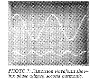
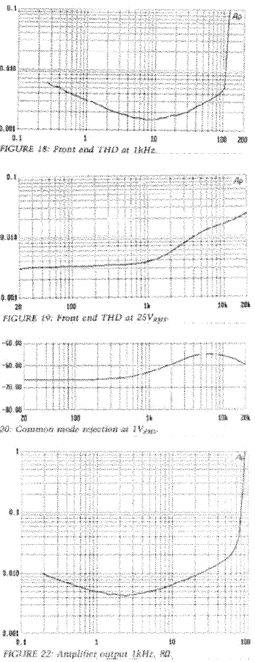
Insofar as the front end can be operated without the output stage, Fig. 18 shows its intrinsic performance with distortion measured against the equivalent output wattage into 8ohm at 1kHz. The distortion versus frequency for the front end at an equivalent of 78W output is shown in Fig. 19. The curve clearly shows the circuit's dominant roll-off pole, which begins at 1kHz and is due to MOSFET capacitance. Photo 7 displays a distortion waveform showing phase-aligned second harmonic.
Figure 20 shows the front end's common mode rejection. The CMRR is the front end's measured ability to null the noise on a balanced input. This figure generally needs to be - 40dB or more, and we typically got - 65dB without matching resistors and capacitors on the input networks. The deviation at high audio frequencies is the result of lack of matching on the input capacitors. [Norm calls me up quoting the latest astronomical CMRR figure he gets by matching the resistors and using tiny trim capacitors. I believe 30,000:1 is the latest figure. - Nelson Pass]
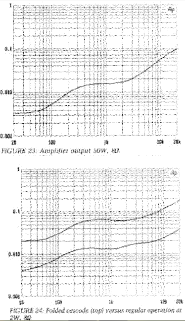
Figure 21 shows the output stage performance when operated without feedback, which is measured with the value of R81 at infinity (i.e., no R81 at all). This figure is quite monotonic, rising to about 0.3% at rated power and resembling tube amplifier performance.
Figure 22 shows the amplifier operated stock, with distortion plotted versus output level at 1kHz.
Figure 23 shows the output distortion versus frequency at 50W.
Figure 24 shows the results of operating with the folded cascode option. Calculation predicts that about one quarter as much open loop gain would be present with folded cascode, and this is confirmed by the two curves' X4 offset. This data is presented to satisfy curiosity, and is not meant to indicate performance quality as such.
As you can see, the performance is respectable enough, but nothing to write home about. Those of you familiar with tube equipment will note
phase response. The amps tend to sound colder and more clinical, with loss of important subjective qualities.
If you decide this amplifier sounds good, then you must question whether THD, TIM, and the host of other bench criteria and marketing jargon are valid to real listening, since the measured performance is not great in any of the bench categories.
The output voltage should be near zero, because there should be insufficient drive to put Q3 and Q6 into conduction. You should see no output signal. Now check the DC voltages across R7 and R8, which should be at a small fraction of a volt. If the voltage is greater than 0.5V, or if you see 2V of output signal, decrease P1 and P2 by turning them counterclockwise. When the DC voltage across R7 and R8 is less than 0.2V and the output is near zero, you can increase the Variac power to full voltage (120V AC).
The DC voltage across R7 and R8 should still be less than 1V. We will now repeatedly adjust P1 and P2, initially increasing (turning clockwise) and balancing their values until the output offset voltage is low, the output signal is 2V or so, and the DC voltage across R7 and R8 is about 0.8V.
Initially, as you slowly increase P1 and P2, you will see the waveform appear with first one peak and then the other. The sine wave will appear with a glitch, or crossover notch, at the zero point. As you alternately increase P1 and P2, the waveform will clean up and, as the voltage across R7 and R8 approaches 0.9V, the waveform will become clean.
Once this occurs, the front end is very likely to be operating properly. Continue to run the front end circuit at full voltage. Verify that + REG and - REG are at + 50V and - 50V, respectively. The voltage across R7 and R8 will drift upwards slightly as the MOSFETs warm up, and the DC offset voltage will also drift slightly.
Turn up the source until the output clips, observing the full + 45V and - 45V swing and symmetric clipping of the front end. Take the oscillator level down to nearly zero, and begin observing the DC drift at the circuit output while monitoring the voltage across either R7 or R8. As the bias and circuit offset drift with warm-up, you can adjust P1 and P2 to bring the offset to zero and the voltage across R7 or R8 to 0.9V. The most effective way is to correct the error only halfway, and then let the temperature and drift settle out again. If you set it straight to the value you wish, it will often overshoot, so approach the proper values by halves.
Ultimately, we will want the voltages across R7 and R8 to be about 1V, although this is not a critical value. By setting it at 0.9V for now, it will typically rise to 1V in a warmed-up amplifier environment. You should be prepared to make final adjustments to the finished amplifier after one hour or more of warm-up.
Set the output offset voltage to < 50mV DC, and readjust it to less than that when the finished amplifier has been running for at least an hour after the last adjustment to its output stage bias. It will generally hold this figure with drift of only 20mV or so after warm-up.
Verify that the DC voltage across + DRV and - DRV is about 7V. If it is greater than 8V, you may have a problem (check to see that P3 is set at maximum resistance), or you may simply need to decrease the value of R80 from 3.3 to 2.7kohm. In any case, the bias voltage should not exceed 8V when you initially fire up the amplifier with an output stage attached, or it may draw excessive current. In actual operation, the DC potential across +DRV and - DRV will be about 9V.
Keep in mind some caveats: we have not provided any protection against a shorted output or static discharge on the input. Although the test amplifiers have survived a short test, we do not recommend shorting the output. Theoretically, it is possible to zap the input with static when
some similarities, except at low frequencies where the design does not suffer transformer coupling.
This amplifier has quite a bit of available output current. It will typically run out at about 70A peak into 0.1ohm loads. If you perform this test, be prepared to replace output devices, or at least fuses. The 12 devices in parallel on each bank are rated at pulses as high as 36A each, for a maximum of 420A. You will never see that, however, not only because the voltage drop through the devices and their source resistors will exceed the supply voltage, but also because Z3 and Z4 will reverse and forward bias when each device is conducting around 6A.
Theoretically, this will place some protective limits on the output current. Here is a caution against setting high output current as a criterion for quality, as seems to be so popular these days. Nothing is wrong with it per se unless, as with other specifications, the design process is perverted into satisfying this one goal. A number of manufacturers have introduced "high current" amplifiers, and many have achieved higher current with triple Darlington output stage topologies. These deliver higher current, but also add greater complexity to the transfer curve and