A75 Part 1
Norman Thagard & Nelson Pass
Introduction
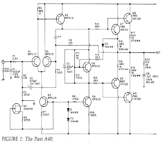
READERS' REQUESTS FOR more power are reasonable, but not interesting enough to justify another article. Hanging some output transistors on the original and beefing up the power supply is best left as an exercise to the reader. While the A75 delivers more power, particularly into low-impedance loads, that is not the primary goal of this project. We wish to introduce more advanced concepts in amplifier design, including balanced inputs, dual differential inputs, true DC response, cascode and folded cascode operation, tiered and regulated supplies, operation with and without feedback, and details of designing with the new generation of power MOSFETS.
As a more complex and advanced project than the A40, it requires more in the way of matching parts and adjusting potentiometers. While the signal path topology is very simple, the circuit taken as a whole is not, and we believe it is important that the enthusiast undertaking this project gains a significant understanding of the function of the individual circuit elements and their contribution to the whole.
Our intent behind this article is design exposition. We want to approach it in such a way that the reader understands the how and why of the design decisions and some of the alternatives. You might be surprised to discover how many decisions are arbitrary, how many are reasonable, and that even better alternatives exist. We hope that by gaining an understanding of the operation of each subsection of the circuit and its relation to the whole, you will fully appreciate the amplification process and possibly go out and design something on your own.
Historically I have found myself competing in the marketplace with some of my own work. If you learn how to design amplifiers here and are crass enough to market them and snatch the bread out of my
mouth, please don't call me up to tell me about it. [Nelson Pass]
We will start by assuming that you know what voltage, current, capacitors, resistors and diodes are. If you don't, then we suggest you find out and come back later. The only other parts in this amplifier to worry about are MOSFETS, so let's start with them.
How MOSFETs Work
The MOSFETS we are dealing with are three terminal devices which are used to control electron flow in a circuit. Two of the pins (the source and drain) pass the current, and the third pin (the gate) is used to control the current (Fig. 2a). The control of current, as seen from the outside, is accomplished by placing a voltage on the gate relative to the source pin. In the case of the N- Channel MOSFET, which approximates tube operation, increased current flows from the drain through the source in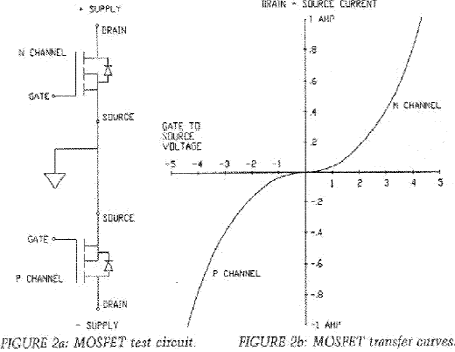 response to positive gate voltage, with respect to the source voltage (fig.2b) If you wish more current, make the gate-to- source voltage more positive (for less, make it less positive). Conduction in the N-channel MOSFET will start generally at about 4V: less than 4V, no current; more than 4V, current flows.
The N-channel type's opposite number is the P-channel type, which is the same but with all the voltage polarities reversed. The drain is generally at a negative voltage with respect to the source, and current flows as the gate voltage becomes negative with respect to the source(Fig. 2b).
In both N- and P-channel it is of interest to know at what rate the current will change with respect to the gate-to- source voltage. This figure is called the transconductance, and tells you how much change in current
to expect for a change in gate voltage. It is generally expressed as mhos (the opposite of ohm), because it describes a reversal of resistance. An ohm is volts divided by amps, and a mho is amps divided by volts so that transconductance is defined as change of current for a change of control voltage. A device having one mho ransconductance will increase its current by 1A for each additional volt on the gate.
Two more points are of interest. First, the MOSFET's construction provides for a reverse bias diode across the drain to source pins, which occasionally is convenient. The second point is rather important from a reliability standpoint: a rather strict limit specifies how much voltage you can apply to the gate before it will break. In our MOSFETs the limit is about 20V. Exceed it and you will need another MOSFET. Static
How to Use a MOSFET
A MOSFET (or some other transistor for that matter) has three pins, and there are only three ways to use it. Since this amplifier will use all three, we will describe them in some detail. Figure 3 shows the three ways to use an N- channel device, each referred to by a "common pin" name, which is that device pin which does not carry signal voltage.
The first use is common drain operation, also known as follower operation. It has current gain but no voltage gain. The input signal is presented at the gate, and the output comes from the source as nearly the same as the input voltage, but shifted - 4V or so. The second is common-source operation, in which we have both voltage and current gain. The input is at the gate, and a phase inverted output signal appears at the drain. The load for the transistor is shown as a resistor here, but can be some other, possibly more complex, load. 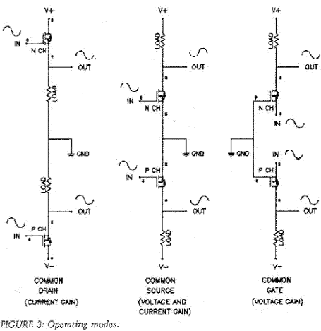 The third way to use a MOSFET is with common-gate operation, which has voltage gain but no current gain. Input appears at the source; output appears at the drain. This connection is most popularly used to form cascode operation, in which a common-gate device shields a commonsource device.
Simplified Design
Since we have covered basic operation of the devices, we will now construct the amplifier circuit one piece at a time. In Figs. 4-9 we will present the circuit adding features and complexity, explaining the additions and changes as we go. Components which receive a designation in the drawings will be permanent fixtures in the series, while others which have values but no number are temporary, and will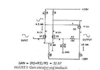 pull down the output of Q3, which by itself can supply only positive voltage and current, and it allows for negative output, providing "bias" for Q3 and placing it in a useful operating region.
We have discussed the three ways to use a transistor, and you may wonder what usage the differential pair is. Well, it is all three types depending on how you look at it. Q1 amplifies input presented at its base in common source, and the signal comes out its drain, as does Q2. But at the same time, Q1 follows the input signal in common-drain mode to drive the source of Q2 in common-gate mode, and vice versa. Confused? Well, don't worry about it. A differential pair is a differential pair, and everything else will neatly conform to our three categories.
The circuit of Fig. 5, is a simple op amp. There is one fundamental thing to know about op amps: they do everything they can to maintain the two input pins at equal voltage. Almost all circuits with op amps get the result they want by satisfying this condition. When they want gain, they use dividing networks to scale down the true out put voltage for presentation to the minus input, as in Fig. 5, where the gain is given by:
(R2 + R3)/R2
which is
15,475/475 = 32.57
Figure 6 shows the differential amplifier used in a manner in which the input networks amplify the difference between two input signals, and 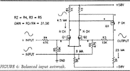
 source as the illustrative case, we note its operation as follows: Resistor R12 feeds about 4mA current from ground to the zener diode Z2. The current is calculated as (VSUPPLY - VZENER)/R12.
In selecting R12 we note the current we wish going through the zener, keeping in mind that the dissipation on the resistor R12 is V²/R12. R12 will generally be a 1/4W resistor, but we will want to run it at less than this, so with a 9. 1V zener diode, the supply voltage (50V) - 9.1V = 40V, which gives a wattage of 1600/R12. A resistor value in excess of 6.4kohm is required. If we use 10kohm, we will have adequate margin and will get about 4mA of zener current. The zener diodes we have chosen are rated as high as 20mA, but that runs them hotter than we like.
As we move toward lower zener currents, the zener diode will become noisier, until at about 0.5mA or so it will become a usable noise generator. At 4mA we will not see too much noise, and we can filter out the noise with the capacitor C4 you see across the zener diode.
What's the Connection?
Now that we have an acceptable voltage source to use as a reference, we will use it to drive our current source. MOSFET Q8 will drive resistor R10. Since about a 4V drop exists between the gate and source (the turn on voltage of the MOSFET), the source voltage will be about 9. 1V - 4V, or approximately 5V. This voltage, divided by the value of R10, will give us the value of the current flowing through Q8 (roughly 10mA). This
While this results in less gain, it allows more speed in many applications and is very popular in ultra high-speed circuitry, particularly video drivers. In this amplifier the speed will not be an issue, but the cascode connection can be used to effectively eliminate one gain stage from the amplifier's topology, resulting in greater stability and purer audio performance.
We have set up this circuit so the differential pair outputs are connected in this fashion, and you may optionally operate the circuit as folded cascode by using capacitors C5 and C6 and resistors R21 and R22. The minimum values of R21 and R22 will be about 75ohm, in order to present the Q3 and Q6 gates with some resistive impedance to prevent oscillation.
If you use this connection and high frequency oscillation results, then you will want to increase R21 and R22 to 100ohm or so. At these values, Q3 and Q6 will be operated at unity gain, and the contributions of both transistors of each differential input pair will be the same in the currents flowing through Q9 and Q10. This output current swing will be at plus and minus 10mA, a 5mA contribution from each of the input transistors. At the output you will see a plus and minus 20mA swing, reflecting the contributions of both circuit halves.
As you increase the values of R21 and R22 above 75ohm, you will see an increase in the loop gain, as Q3 and Q6 begin to dominate the front end output. When R21 and R22 are increased to about 270ohm, the drive from the input pair will allow the full plus and minus 40mA swing on the 20rnA bias through Q9 and Q10.
With R21 and R22 set at very high values, say 10k or more, values of R1 and R6 will dominate the operation of Q3 and Q6, for a gain at this stage of about 20. We suggest you try different values and evaluate the performance sonically. You will not need to readjust P2 and P1 potentiometers, since they will set a constant value for the DC bias of Q3 and Q6.
But Is It Aerobic!
Later we will show some performance data from operation in the folded cascode mode. Using this mode effectively eliminates the intermediate gain stage from the amplifier, resulting in higher measured distortion due to the lower open loop gain of the circuit (less feedback), but offering a different sonic signature by virtue of the simpler gain path. It is an interesting effect, and we leave the exercise to the reader. The circuit will operate properly and be stable over the range of R21 and R22, from about 75ohm to open.
We now have a workable amplifier, although it will not drive a low
extra speed, each of us changing his mind at least once. In the end, we decided to dispense with the driver transistors for the following reasons:
1. Simpler is better. The fewer transistors the signal goes through, the better, all things being equal. Removing drivers also gives the amplifier greater frequency stability, making it easier to compensate and posing fewer problems for amateur constructors.
2. The arguments for high speed in audio don't make much sense. Tube amplifiers are not fast, and so do not suffer this complaint. TIM is not particularly at issue, since we are absolutely minimizing the amount of feedback in this design. As a theory which explains everything, Pass considers that it has fallen far short of its promise, and is barely applicable. Most of the commercial designs featuring very high speed have not sounded very good, and none have gained commercial popularity.
3. Contrary to popular myth, there isn't much speed in audio signals. Previously published measurements indicate music slew rates rarely exceed 1V/uS, and even then never see more than a couple of volts/uS. Most of the material we listen to is about 0. 1V/uS, or less.
4. We didn't give up much speed anyway. The project amplifier's actual slew rate came out at about 30V/uS, which gives a full power CD bandwidth margin of about 6:1. Using drivers will get us into the range of about 100V/uS, which is a faster, but not an astronomical, improvement.
The Whole Circuit
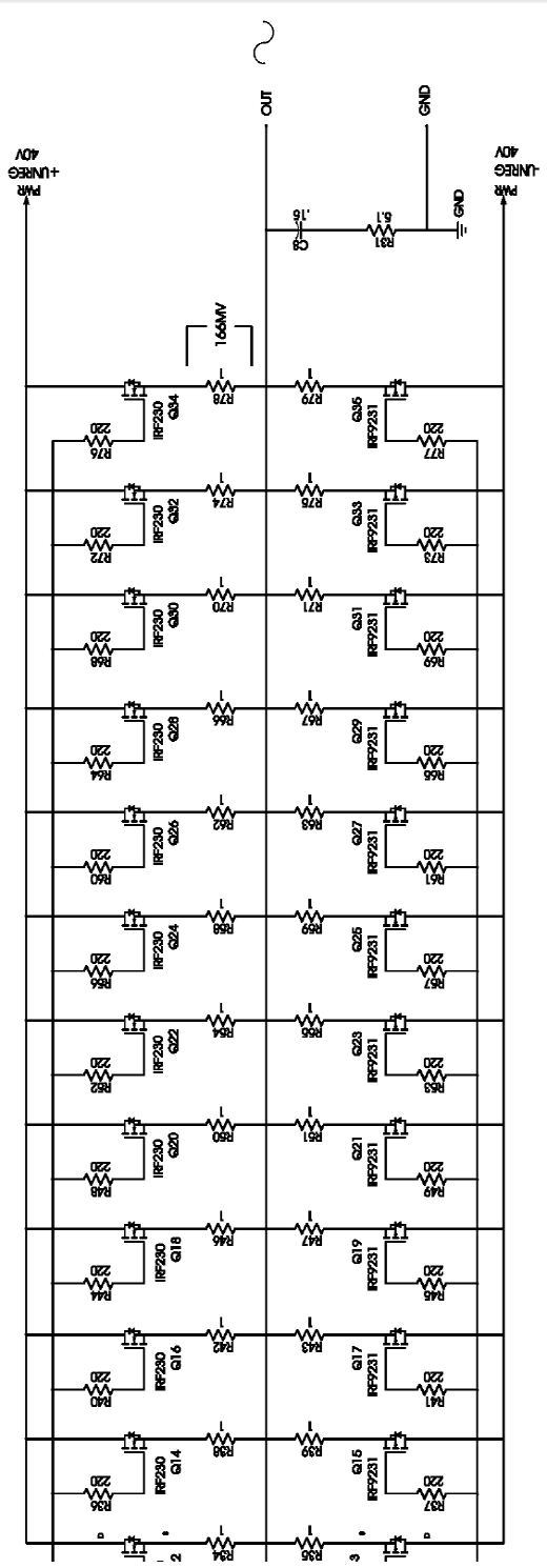
We leap now to Fig. 9, which presents the entire circuitry for one channel of the amplifier. Its formidability is the result of parts repetition; we will go through the additions one at a time.
The first things you will notice are two banks of 12 MOSFET output devices arrayed in parallel. They are configured for common-drain (follower) mode, where they contribute only current gain, not voltage amplification. Arranged in a complementary fashion with the P- channels on the negative side of the circuit and the N-channels on the positive side, each device has resistors at its source pin and in series with its gate. The resistor on the gate prevents self-oscillation, as you will recall, and the source resistor ensures proper current sharing between output devices and temperature stability.
Considerable hype permeates the marketplace regarding MOSFETs' intrinsic ability to share current in parallel, and their negative temperature coefficient. With bipolar transistors, the junction voltage (VBE) for a given current will decrease with temperature, resulting in higher current flow. If the current flow increases enough to significantly raise the temperature, then the junction voltage will decrease further, the current will increase, and thermal runaway will occur in the transistor.
This positive temperature coefficient is responsible for "second breakdown" in bipolar devices, where hot spots develop on the transistor surface and begin hogging the current. Second breakdown limits the usefulness of the transistor at higher voltages; for example, an MJ15024 is rated at 250W at 25V, but only about 100W at 100V. Current hogging
discharge is an excellent way to exceed the limit, and the best way to do that is to pick a cold and dry winter day, shuffle across the nylon carpet in your rubber shoes, and touch the gate of a MOSFET. The second best way is simply to forget to touch earth ground before you touch that part for which you do not have a spare.
That's most of what there is to know. Other reliability details include rated voltage, current and wattage, and what package the MOSFET is in, but you can see these in the catalog. More arcane bits of information include saturation resistance, various capacitances, switching times and such, but if you can remember the preceding description you know 90% of everything about MOSFETs, and 100% of what you need to understand this project. 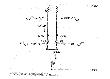 be replaced by something else as we progress.
The first step is to construct an in put stage known as a differential pair: two transistors with their sources tied together, and fed current at that connection (Fig. 4). In this case, current is fed by a 5kohm resistor attached to a - 50V supply. Two inputs are available at the gates, as are two outputs at the drains, which then communicate through load resistances to the positive supply.
The drains present equal but inverted outputs, which represent the difference between the inputs. If both inputs see the same signal, then that signal does not appear at the outputs. It is a differential amplifier, which means any differences in the input signals at the gates are amplified, and common signal is rejected. For this reason, it is extremely useful as the input stage for an amplifier, because you can connect an input signal to one gate and use the other gate to watch the amplifier output.
The Winning Pair
This output watching is called feedback. The differential pair is used to compare input and output, and by amplifying their differences it is used to correct for errors at the output. Figure 5 illustrates this concept, where the differential pair is followed by more gain circuitry (Q3),whose output is then fed back to the gate of one of the differential pair (the minus input). In this case gain is desired, and we use the resistive voltage divider formed by R3 and R2 to fool the input pin into thinking the output is smaller than it really is.
The gain circuitry following the differential pair often has a lot more gain than is really required, but the differential pair will send out just the right amount of signal to get the desired output. In all cases, this output will be such that the two input pins of the differential pair are at equal potential, and the circuit will maintain that condition.
If the voltage at the plus-input pin is varied, the circuit will work to deliver the same voltage at the minus pin. Note that the output of Q3 drives a 2kohm resistor attached to the negative supply. This resistor is used toalso allow for negative feedback. In audio this is known as having balanced inputs, and the gain of this circuit is R3 . R2. Balanced inputs amplify only the differences, ignoring signals and noise which are common to both. The ability to ignore common signal is called the common-mode rejection ratio (CMRR). Audio equipment value lies in the ability to operate with less noise pickup, particularly hum. This project will make use of balanced inputs; the values of the input will need to be matched in order to get a good CMRR figure, so we will set R2 =R4 and R3 = R5.
Double or Nothing
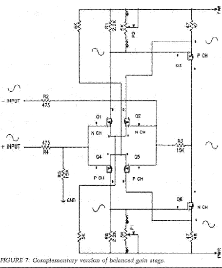
A circuit can have more than one differential pair as inputs. This amplifier will have two pairs: one of N-channel devices and another of Pchannel devices Q4 and Q5 (Fig. 7). The outputs of the N-channel devices head off toward the positive supply, where they will drive the positive half of the amplifier gain circuitry Q3; the outputs of the Pchannel devices will head toward the negative supply, where they will drive the negative half of the circuit, Q6.
In this example, Q6 now effectively replaces the 2kohm resistor we were using in Fig. 6 to bias Q3. Q3 and Q6 will operate in opposition to each other, one onducting less current as the other conducts more in order to create varying voltage output at their connected drains, all under control of the differential pairs at the input.
We have adjusted the value of R1 and added R6, which performs the complementary function on the negative side. In parallel with both these resistors are potentiometers to adjust their values. This allows us to trim the amount of current which will be flowing through Q3 and Q6, and is necessary because of the variations in gate-to-source voltage characteristics of individual transistors. We don't want too much or the transistors will run too hot, and too little will create excessive distortion. Later, we will also use these trimpots to adjust the amplifier's DC offset voltage.
Resistors R7 and R8 placed at the sources will help stabilize the gain of Q3 and Q6, and will later provide current sensing for both adjusting and limiting. We want to set the voltage across these resistors at about lV, giving DC current flow through Q3 and Q6 of about 20mA.
Some Like It Hot
We will now deal with how the differential pairs receive their operating current. You can deliver this current through the 5kohm resistors (fig. 7), but it will not be very constant, and will fluctuate with signal and supply voltage. Differential pair operation depends on an unvarying current supply, and an active constant current source will deliver better performance than a resistor.
Figure 8 shows the addition of two such current sources, one for the P-channel differential pair formed by Q7, and its complement for the Nchannel pair formed by Q8. Taking the N-channel current will depend solely on the voltage across the resistor and will be constant enough for our application. The same logic and calculations apply to the P-channel current source.
Our addition of C1 and C2 in the input and feedback networks create a small amount of high frequency rolloff, not enough to significantly affect the audio signal, but enough to help keep the local radio station from being received. In order to preserve common-mode rejection, the value of C1 and C2 must be equal, just as R3 equals R5 and R2 equals R4.
If we examine the performance of the circuit in Fig. 7, we find some performance limitations associated with distortion and speed. The rapidly varying voltages appearing on the drains of Q3 and Q6 cause transconductance variations, and also charge the capacitances of the MOSFET junction, resulting in slower response.
We can remove quite a bit of this by using a cascode connection, by adding common gate MOSFETs Q9 and Q10 (fig. 8). They do not add current gain, but merely shield Q3 and Q6 from the output voltage fluctuations. In doing so they reduce distortion and improve speed of Q3 and Q6, while contributing very little of their own characteristics. They can be controlled (biased) by the same zener diodes which were used to control the current sources, which sets them up to present about 5V across Q3 and Q6.
In Fig. 8 you should also note that we have suddenly added resistors in series with the gates of most of the MOSFETs, which are such wideband devices that, given any excuse, they will form excellent selfoscillators. One such excuse is a low impedance on the gate, so it is always wise to insert some nominal resistance in series with the gate of a MOSFET, which otherwise might see a low impedance at high frequencies. This will not be necessary for Q3 and Q6 which already see the resistances of R1 and R6, but it will be necessary elsewhere, so we add resistors R13 through R20.
Less Is More
Now that we have implemented a cascode connection on the voltage gain stage, we will digress to explore a variation of cascode operation: folded cascode, which is a method of using the heretofore unused differential outputs at the drains of Q2 and Q5. Figure 8 illustrates this technique, where the output of Q2 is inserted into the connection between the drain of Q3 and the source of cascode device Q9. The output is the right polarity to drive Q9 by itself, without Q3's output drive. If we place a capacitor across R1 so as to remove the AC portion of the drive to Q3, then Q3 behaves as a constant current source and no longer contributes gain (or distortion or delays) to the circuit. The drive in this arrangement comes solely from Q2, instead of the combination of Q1 and Q3. 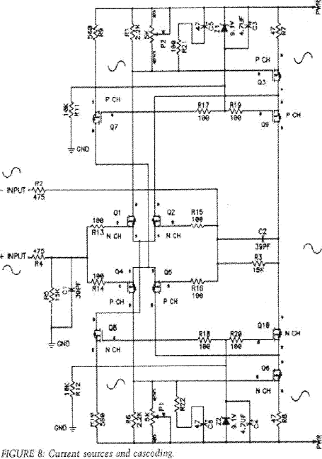 impedance load. Without modification it would be a perfectly acceptable line gain stage for a preamplifier, and you might choose to use it as such.
If you want to drive impedances down to an ohm or so, you will need an output stage. For this we will use a bank of complementary (both P- and N-channel) MOSFET power transistors operated in the common-drain (follower) mode. At this stage, most designers consider using driver transistors prior to the actual output transistors.
In bipolar designs they are essential due to the high current demands of the output stage, but MOSFETs do not have that requirement, due to extremely high-input impedance at audio frequencies. The justification for the additional gain stage would be the extra speed obtained by driving the capacitance of the output stage transistor gates, which are about 80- l00pF each.
Speed Trap
We went back and forth trying to decide whether or not to use drivers for
due to the positive temperature coefficient demands that parallel bipolar designs use emitter resistors to force current sharing.
If you believe what you read, you think that MOSFETs don't have any of these problems, but that is not quite true. While touted as having negative temperature coefficients, they actually have positive temperature coefficients up to rather high currents. In the case of this amplifier's output devices, the coefficient is positive up to about 3A, so that under average conditions the bias will tend to wander upwards slightly with increased temperature.
Mix and Match
In this and other linear MOSFET designs using parallel transistors, the output devices need to be carefully matched with regard to the VGS at their idle current. Devices vary considerably, and a difference as high as 0.5V will result in some transistors doing all the work and others doing nothing.
Both problems are reduced with the use of matched devices. We also use source resistors, which tends to equalize their characteristics. We have chosen relatively large values for source resistance (1ohm), but this is not a problem since we have lots of parallel devices, and in a Class A circuit all 24 devices will only add about 0.04ohm to the open loop output impedance. Proper current sharing will be ensured at 1ohm, and will add to the bias stability of the output stage.
Using a resistor as large as 1ohm is a benefit when an output device shorts, since the current (and thus damage) can often be limited to the failed device without destroying the remainder of the output stage. We have built test samples of this output stage with source resistance as low as 0.33ohm without problems, and you can try lower values if you like, as long as the outputs are well matched.
We will need to bias these output devices into their linear Class A operating region, and for that we will use the voltage source provided by the circuit around Q11. If you have ever built an amplifier using bipolar devices you may be familiar with the VGS multipliers bipolar counterpart, the VBE multiplier.
Remembering the conduction requirement that VGS will be about 3.5-5V in a MOSFET, we arrange resistors R80 and potentiometer P3 so the potentiometer will see the VGS of 4V. In meeting this condition across its resistance, a particular constant amount of current will flow through P3 and this same current must come through R80, setting up a constant voltage there. The bias voltage across Q11 is equal to the two voltages added together and is given by the formula:
V (R80 + P3)
where VGS = 4V. To bias the output stage into conduction we will need about 9V across Q11, or about 4.5V for the P-channel bank of outputs and 4.5V for the N-channel bank.
We put the potentiometer P3 across the gate-to-source pins on the bias MOSFET because if it fails resulting from an open wiper connection, it
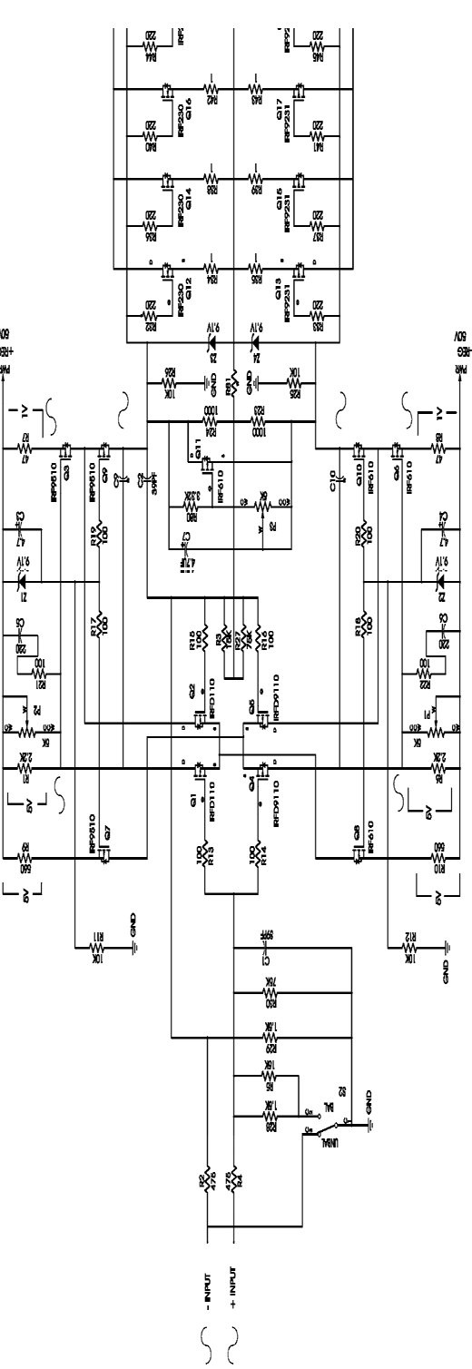
will unbias the amplifier instead of smoking it. Placing capacitor C7 across Q11 ensures low impedance and a passive characteristic at high frequencies.
Decisions, Decisions
Let's notice a few other things about Fig. 9a and Fig. 9b. Zener diodes Z3 and Z4, which go from the drive to the output, protect the output gates from overdrive.
At the output node we see an RC load network of R31 and C8, which helps stabilize the amplifier when it looks out at the real world. It damps out some of the strange high-frequency resonances which develop in driving real loads and cables. This network has been employed on every (working) solid state amp ever made.
The feedback loop attachment, formerly from the drains of Q9 and Q10 to R3, now goes through two resistors, R23 and R24, because the bias circuit removes the nice neat feedback takeoff point. Instead of a simple output for the front end, we now have two outputs which share the same AC voltage but are 9V DC apart. R23 and R24 divide this 9V in half and give us a nice midpoint voltage, which is close to the actual output voltage.
Note the addition of new resistor R81. Here you will have some options: do you wish to run feedback around the output stage? None? All? Partial? Your choice of resistors for R81 will give you this adjustment range. R81 = 0 will mean feedback is taken 100% from the output stage, at the output of the amplifier. R81 = infinity (open) will mean no feedback is taken from the output stage, but rather from the front end output only through R23 and R24. The output stage and the amplifier's output will not be included in the feedback loop.
Or you can do something in between. When the parallel values of R23 and R24 equal R81, you will be taking 5096 feedback from each. As R81 gets larger, you have less feedback around the output stage; as R81 gets lower, there is more. The distortion figure will go down as R81 goes to zero, because you are applying feedback correction around the output stage.
Later on, we will show a distortion curve resulting from operating the amplifier without feedback around the output stage. Maybe you want that feedback, maybe you don't. Maybe you can hear it, maybe you can't. In either case, let us know!
Raising the Stakes
As you increase the value of R81 from zero, you will find it reduces the common- mode rejection of the balanced input. If you are not using the input as balanced (by shorting the minus and simply driving the plus input), then it doesn't matter. If you don't need very high common-mode rejection (and generally we don't in order to get quiet performance), again it doesn't matter. But if you wish the utmost in common-mode rejection, all your impedances must match exactly, which means reducing the parallel value of feedback resistors R3 and R27 by an amount equal to R81, and adding yet a third resistor in parallel with them.
interact with high-impedance networks. To prevent distortion resulting from this at high frequencies, we should keep the resistor values as low as possible.
Gang of Four
Figure 10 shows the equivalent network when operating in balanced mode. On a differential amplifier with such a network, there are four ways of looking at the input impedance: the common mode input impedance, the positive input impedance, the negative-input impedance, and the differential-input impedance. The common-mode input impedance, seen by signals and noise which are identical at the two inputs, will be R4 in series with the parallel combination of R5, R28, and R30 (475 + 1.34k= 1.815k).This input impedance is seen individually at both inputs for common-mode signal and noise.
The equation for determining this value is sufficiently complex that we suggest you use a large-value trimpot (start with 1Mohm) and adjust for maximum CMRR. In general, however, 40dB of common-mode rejection is sufficient to keep a home system's noise as low as the noise you see on the test bench. This amplifier will typically exhibit 60dB rejection without trimming input resistor values, but like high damping factors, high CMRR offers diminishing returns.
Two new capacitors, C9 and C10, add some lag compensation in the event that a particular choice of components and layout are not adequately stable. We offer no values, since we did not use them in the amplifiers we built, nor have we encountered the problem in a range of prototypes. If necessary, your choice of capacitors will be for whatever prevents high frequency oscillation, and may range from 5 to 39pF. If oscillation occurs, consider raising the values of the gate resistors on the MOSFETs first.
The two new resistors, R28 and R29, in the input and feedback networks ensure amplifier stability in case the negative input is not terminated in a sufficiently low impedance. If you leave the minus input connector open, the amplifier gain would fall to less than one, which is a problem in itself, but it also may cause frequency instability at such a low loop gain. The addition of R28 and R29 ensures stability even when the minus input is left open.
Swing Things
Maybe you want to ask, "What are those new parts and that switch doing at the input?" The switch makes it easy to go from a fairly lowimpedance balanced input mode to a fairly high impedance unbalanced input. In unbalanced mode, the switch shorts out the negative input and disconnects R28 and R5, leaving R30 connected to ground to serve as a 75kohm input impedance. When the switch is in balanced mode, it connects R28 and R5 to ground. In order to balance out the addition of R30 at the positive input and preserve CMRR, we have to add R27 in parallel with R3 on the feedback loop.
Another thing to note about Fig. 9: the output stage power supply is not the same as the front end supply. Using a separate and regulated front end supply to reduce noise and modulation effects from the output stage is preferred, and provides performance stability at varying line voltages. With front end supply regulation you see lower noise and distortion, and also less DC offset and bias drift.
Because of the 4-5V gate-to-source voltage drop on the output stage follower transistors, the front end must swing about 5V more than the output stage supply rails in order to get maximum efficiency. (And with a pure Class A amplifier you want all the efficiency you can get.) The front end itself will swing to within 5V or so of its own supply, so we want a front end power supply whose voltage is at least 10V higher than the output stage rails.
A word about balanced inputs: this amplifier achieves balanced input operation without the use of external active circuitry, which is preferred. The price we pay for this is the lower input impedance required for high performance The input MOSFETs have finite capacitance, which will
Drive, He Said
A good way to drive this network is also shown in Fig. 10. The positive input is actively driven by the source circuitry of whatever preamp you choose to use, assuming it will drive 1.8kohm. The negative input is passively terminated at the source-to-ground through whatever impedance matches the output impedance of the active source. This gives full value to the noise rejection capability of the balanced input, and avoids having to drive a particularly low impedance negative input.
Of course, you can drive the negative input as you like, and its input impedance is not significantly lower than the 300ohm representing half of the 600ohm balanced commercial standard.
If all these low impedances frighten your preamp, you can always run
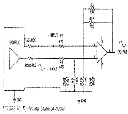
At the positive input, this is also the impedance seen by the signal, since the positive-input network is not attached to the amplifier output, and the impedance is passive. At the negative input, however, both the network's passive impedance and what is happening at the output form the input impedance.
Assuming that the differential signal input is equal in amplitude but opposite in phase at the two inputs, we see that the operation of the feedback loop will work to create equal voltages at the gates of the differential pair transistors. In the example of a positive 1V at the positive input, the gate voltage will become 0.738V. This same 0.738V will also appear on the other side of the minus input of 475ohm resistor R2; if it is being driven at - 1V simultaneously, we see that the current through R2 behaves as if R2 were 475/1.738, or 273ohm.
Under these conditions, the input impedance of the negative-balanced input is less than the input resistor, and must be taken into account. The differential impedance seen at the balanced inputs is the sum of the input impedances, which is 2.088kohm.
the circuit in unbalanced mode by throwing the switch, in which case the input impedance will be slightly higher than 75kohm. Alternatively, you can scale these resistor values upward with some resulting degradation of the high frequency distortion figure. Scaling the values exactly is unnecessary, the only requirement being that corresponding values on the positive and negative input networks be matched.
Stay Tuned
Part II of this article will be published in the next issue of TAA. Power supplies, components, chassis, output stages, and testing are just a few of the topics which will be covered.


