Zen I/V Converter
Nelson Pass
Introduction
Thirteen years ago Pass Labs launched the D1, a dedicated Digital to Analog converter for high end audio. It was based on balanced PCM63 DAC chips with a current source output, which requires a separate current-to-voltage converter (known as an I/V) to turn its output into the voltage to drive other line level audio equipment. We didn't care much for the op-amp based solutions seen in the manufacturer's application notes and decided to approach this part of the circuit much differently.
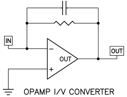
The PCM63, like other current output DACs, favors driving a very low impedance, preferably ground. You can easily create a virtual ground at the input of an inverting op amp circuit, as seen below:
This is your classic I/V approach, where the gain of the circuit is proportional to the value of the resistor (1 Kohm = 1 volt per mA) and the input voltage is held very close to 0 volts, giving a very low input impedance. The capacitor is a filter designed to smooth the “stairsteps” in the output of the DAC chip which occur at the sampling rate, which for CD's is ordinarily at 44 Khz. The intent of the filter is to remove the sampling rate and its surfeit of higher frequency noise so that they don't create problems for the subsequent amplifying equipment and listeners who might be able to hear that high. Most designers opt for multiple poles of low pass filters, so you will see more capacitors in subsequent gain stages of the DAC.
Without wanting to get into an argument about the pros and cons of op amps in audio circuits, I must point out that this sort of usage of an op amp places it at the greatest possible disadvantage – operation at unity gain with a mix of audio and high frequency noise.
Why would I think this, you ask?
Designed with high open loop gain in mind, op amps become marginally stable as the feedback is maximized, which occurs when an inverting loop is driven by a high impedance current source as above.
When I was a young sprout playing with op amps, I noticed on occasion that they simply sounded bad, but if I adjusted the rail voltages down or raised the gain they suddenly popped back. After I acquired some decent test equipment I could see that they were suffering from oscillation, and that the bad sound was accompanied lots of distortion and high frequency noise. At that point I learned to take op amp manufacturer's claims of unity gain stability with a grain of salt (and improve my layout and power supplies).
Later I noticed that I was hearing differences depending on the relative gain (and feedback) of op amp stages even when there was no oscillation. It appeared as if simply approaching the point of instability created issues that didn't show up on the distortion analyzer. Since then, I have learned to give potential feedback issues a wide margin.
On another occasion I designed an experimental amplifier that proposed to use a high frequency bias (similar to tape recorders) in an amplifier output stage as a means of reducing crossover distortion. The result measured reasonably well, but the sound was awful. I concluded that mixing high frequency tones with audio and feedback is a bad idea.
I encountered another such instance in a vinyl cutting session with Telarc where an ultrasonic tone of low amplitude was accidentally introduced into the system. The resulting record had issues that the producers could hear plainly on the pressing (Yes, Robert Woods and Jack Renner had excellent ears) and no one could guess at the problem, but I played the record into a spectrum analyzer and identified the tone. They remastered it from scratch.
And that's why I think these things.
Given the idea that the I/V converter above is inviting trouble, what can we do?
We can use a gain device in its most absolutely linear and stable mode: Common-Gate (or Common-Base, Common-Grid). In other words, we should cascode the output of the DAC chip. In Common-Gate mode (in the case of a Fet) we attach the Gate to ground (or at least an AC ground) and send the input to the Source pin. The Source pin has is a relatively low impedance, more or less the inverse of the transconductance of the gain device, which satisfies one of the conditions that a current source DAC is looking for. Given the nature of the Fet and the high output impedance of the DAC chip, all the current output of the DAC will appear at the Drain of the Fet and will be driven through some value of resistance to deliver an output voltage.
The very nature of Common-Gate mode insures the absolutely lowest distortion and widest bandwidth possible. It is not often used because its input impedance is very low, but in this case it's a natural.
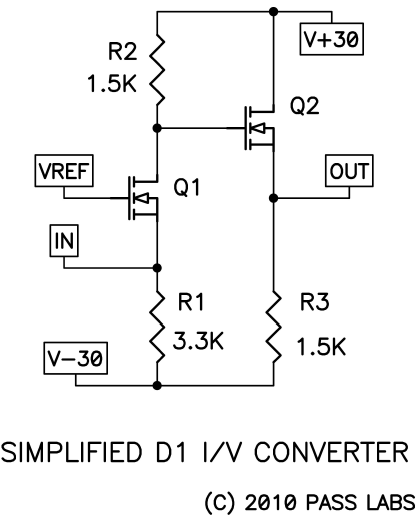
The D1 used a Mosfet in Common-Gate mode as seen below in a simplified circuit:
In this circuit the input occurs at the Source of Q1, and we see that Q1 is biased to approximately 10 mA by the current through R1 attached to the negative 30 volt supply. Vref is a DC reference voltage adjusted so that the Source pin of Q1 is at 0 volts. The non-inverted output signal is seen at the Drain of Q1, where the signal current develops the output voltage across R2, which is then simply followed by Q2, appearing at the output. If you don't need a low output impedance, you can delete Q2 and R3.
This works very well, and the D1 remains highly regarded today.
Interestingly, it took a long time before anyone seemed to understand what was going on. I showed it to a “designer” at a major DAC manufacturer at the time and he told me that he didn't see how it could possibly work, and he wasn't the only one. Presumably he needed to see it in a manufacturer's application note.
Since then a number of DIYers have caught on and there are a couple of variations on the internet, and at least one manufacturer using a variation on this technique. A few years after the initial circuit I developed an increased interest in the performance of Jfets in this sort of application, and it resulted in a nice little circuit.
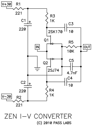
Recently I offered a prize on www.diyaudio.com for the best suggestion for the next DIY project, the prize being the project, and this article being that. Below I present the Zen I/V Converter:
I have looked around on the internet, and I have not seen it duplicated by some smarty-pants, but that is no guarantee that it hasn't occurred. Q1 and Q2 are self-biased Jfets operated in Common-Gate mode, taking their input from a current source DAC chip and presenting their output on their drains at R3 and R4. R3 and R4 in parallel set the gain, which is 0.5V per mA input. R1, R2, C1 and C2 are simply passive filters. If you think your 30V supplies are noise free then you can modify or delete them. C3 and C4 capacitively couple the output so that we don't have DC arguments. R5 is simply a resistive load, which you can modify or delete if you like. C5 is the high frequency filter, which you can also modify or delete.
There is no feedback. The Jfets were selected for matched Idss at 10mA, and present a DC offset voltage at the Source about 1 mV, which is plenty low. If you have unmatched Jfets, then I suggest you use a low impedance resistive voltage divider to offset the DC Gate voltage by the required amount. By low impedance, I suggest that the resistor to ground be on the order of 10 ohms or so.
Note that at 10 mA bias, the Fets will end up with about 15 volts Drain-Source. With other Idss bias figures you may adjust the values of R3 and R4 up or down to get this figure. If you want more gain (and I bet some of you do) then you can increase R3 and R4 to 2.2 Kohm each for twice as much, but you then need to add about 10 more volts to each supply rail to arrive at the +/-15 Volt Drain voltages on the Jfets.
The input impedance is the inverse of the transconductance of the two Jfets in parallel, which at 30 mS each comes out to around 15 ohms. The output impedance is roughly the values of R3 and R4 in parallel, and for the example shown that is around 500 ohms.
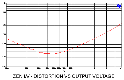
Here is the distortion versus output voltage:
This curve was taken at 1 Khz, and does not vary over the audio band. The values below 0.4V output reflect broadband noise, which in my test setup was below -100 dBV, or 10 uV.
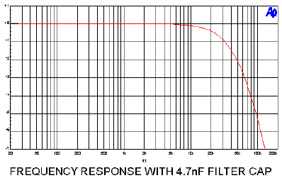
The low frequency performance can be extended arbitrarily simply by increasing C1 through C4 or removing them altogether. Without C5 the bandwidth very high, and with C5 at 4.7 nF, the response starts to decline at 20 Khz. You probably want this, but maybe not. Conversely you may find that you need more filtering. You may add a capacitor from the input to ground, keeping in mind the approximate 15 ohm resistance for your RC calculation, and you may find that you want subsequent low pass filtering after the output.
Here is the response curve of the circuit as shown:
So there we are. Have fun! 
© 2010 Nelson Pass


