The Pass A-40 Power Amplifier
Nelson Pass
Introduction
FLATTERED BY THE opportunity to publish a project circuit, the designer is often beset by seemingly contradictory considerations. On the one hand, it is tempting to design a complex circuit as a demonstration of technical prowess; an amplifier with large numbers of esoteric components performing obscure functions. Such an amplifier might be a smorgasbord of electronic technique, featuring class A operation, cascoding, constant current sources, current mirrors, and extra-loop error correction. It would be fascinating to build and perhaps would also sound good.
On the other hand, complexity is not a good end in itself and a much simpler circuit would suit the needs of the amateur more ideally for low cost, high reliability, and easy construction. Simplicity can often yield sonic benefits, inasmuch as the fewer the number of components in a signal path, the simpler the open loop transfer curve of the amplifier.
The importance of a simple transfer curve accounts partially for the high quality of sound in many tube type devices. Their simple circuitry assures a higher concentration of low order distortions, 2nd and 3rd harmonics and 1st and 2nd order intermodulations, giving them a pleasant musical sound even at relatively high distortion levels. By contrast, the higher order distortions to be found in many poorly biased solid state amplifiers are less musical and thus more detectable.
This effect is similar to one's ability to detect a scraping voice coil on a woofer more easily than a much higher percentage of 2nd harmonic in the woofer. While this is partly due to the unmusical nature of these overtones, it is also due to a fault in the measurement technique which assumes that our ears are average responding, like the meter on the distortion analyzer.
A good example is crossover notch {the amplifier's equivalent of a scraping voice coil}, which is a spike of distortion occuring when the transistors are switching the signal from the positive set to the negative set and back again. Because it only occupies a brief percentage of the operating cycle, crossover notch distortion can occur in very high peaks which then are averaged down to a much lower figure, giving a misleading impression of the audibility.
Does the ear respond to such brief distortions? I don't know, but it is true that amplifiers with nearly identical "standard" specifications can sound different and it seems that low versus high order harmonics and intermodulation are one common key to the sonic disparity.
Fewer elements in series with the signal path also result in wider bandwidth and greater stability, as there are fewer contributions to the high frequency rolloff of the circuit.
PERFORMANCE VS. PARTS
Given then that the circuit should be simple, we must find a way to achieve the exceptional performance as advertised. While we want 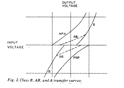 amplifiers. The distortion is inherently lower without the need for cleaning up via feedback, thus class A lends itself well to low distortion performance in a simple circuit with low open loop gain. Fig. 2 shows the transfer curves for a push-pull emitter follower output stage operated in class A, B, and AB modes where the crossover distortion is apparent in the discontinuity of the curve. In class AB, this effect is alleviated by a small bias current, and then is eliminated in class A where the bias current is high.
Fig. 3 shows the open loop output impedance of these stages where the class B amplifier is seen to rise abruptly at the discontinuity, whereas the class AB actually drops at the point where both halves conduct current. The class AB amplifier can be said to run in class A over this small region and will exhibit class A performance at small current levels. The class A curve can be observed to be the smoothest of the three in an effect which can be looked upon as the damping factor of the amplifier multiplied by the amount of feedback employed.
Naturally, this kind of performance has a price tag, and with class A operation, the low efficiency causes considerable energy loss. Class A power amplifiers require large power supplies to handle this energy, but the task is not as enormous as might be imagined.
BEATING THE HEAT
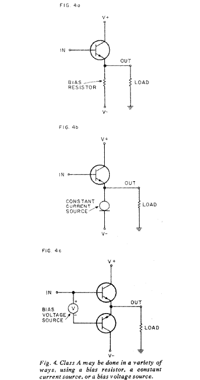
Class A amplifiers have different efficiency factors depending upon the design. The least efficient is the circuit of Fig. 4a, where the transistor is biased by a resistor and whose AC output power to the load is less than 20 per cent of its idling dissipation. Fig. 4b shows the same configuration where a constant current source replaces the resistor, improving the linearity and efficiency of the circuit. The value of the constant current source must be equal to or greater than the maximum output current. For an 80W peak (40W, rms) into 8 Ohms, therefore, the current must be at least 3.2A, which practically speaking means a worst case dissipation of 200W per channel in the idling output stage.
Push-pull circuitry more or less doubles the efficiency of a class A output stage (Fig. 4c) because unlike the constant current sourced design, its idle current need be only one half the peak output current, or 1.6A in the example, for an idling dissipation of about 100W for a 40W amplifier.
At these power levels, we will expect some degree of heat and will need to figure out the amount of cooling required. If we assume a 25° C. ambient temperature, for each channel we will require a heat sink with a .25° Celsius per Watt thermal characteristic. This can easily be made from two .50° C./Watt sinks or four 1° C/W sinks, remembering that air should flow vertically along the fins on the sink and that some free space must be available on all sides of the heat sink, especially top and bottom. With this much sinking, the 100W idling dissipation will raise the sink temperature at 25°C above ambient for a temperature of 50°C.
This is easily handled by the four output transistors whose cumulative dissipating capabilities are 600 Watts at this temperature. The 6:1 safety margin here may cause some readers to wonder if I wear both a belt and suspenders, but in my experience, textbook safe operating areas are somewhat optimistic. In real life circuits with a 2:1 safety margin generally blow up.
HEAT AND ECOLOGY
Contrary to popular belief, class A output stages are not necessarily subject to thermal runaway. Whereas class AB amplifier designers often invest in thermal compensation to correct the delicate bias voltage, class A output stages use a gross bias current without much need for small adjustment. The high bias currents develop significant voltages across the transistors' emitter resistors, reducing the temperature dependence of the bias. In addition, this amplifier incorporates an interesting bias circuit which senses the idling current of a class A output stage while ignoring the AC signal and maintains a constant bias without need for adjustment.
One nice thing about hefty output stages as found in class A operation is that often no protection circuitry is required beyond a fuse because of the excellent thermal capability of the bank of transistors. This same capability yields better performance into demanding loads and holds the transistor chips at a more constant temperature than the flimsier output stages found in class AB amplifiers.
Nevertheless, I must admit that class A operation consumes energy which is converted to the heat emitted by the amplifier. While its consumption is about on a par with a large color television, the ecologically oriented audiophile may wish to operate his class A amplifier only during the winter, when he would otherwise be using his heater, and revert to a class AB design amplifier during the summer.
simple distortion types, we also want a lot less of them, which brings us to the question: what techniques will extract maximum performance from a few parts? In this case I have chosen two very effective approaches: constant current sourcing and class A operation which are combined in a deceptively simple 40 Watt per channel amplifier.
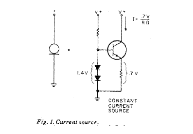
Constant current sourcing is a technique used to achieve high gain and linearity by biasing transistors heavily without loading down the gain as a resistor current source would. A constant current source delivers a specified value of DC current regardless of the fluctuations of the power supply or the voltage swing of the amplifier, resulting in less distortionand noise.
Constant current sources may be formed in a number of ways, one of the most popular being the circuit for Fig.1 where the forward voltage drops of the PN junctions is used as a reference to drive about .7 Volts across a resistor. This voltage across the resistor causes a constant current to flow through the collector/emitter path of the transistor which is independent of the voltage at the collector between saturation and breakdown.
Of particular value in linear circuits, constant current sourcing sets up conditions where the device's operation moves it about its operating point by only a small percentage of its capability.
WHY CLASS A?
Class A operation is integral to the performance in this case, and it is worthwhile to explore why. The primary virtue of class A lies in the smooth characteristics of its operating parameters. The gain transistors are operated in their linear region only, where the distortions are limited to smooth, simple forms, unlike the abrupt distortions created when the transistors in class B output stages switch on and off.
In class A, the transistors are always on, eliminating the turn-on/turn- off delays which characterize the crossover of class B and even AB 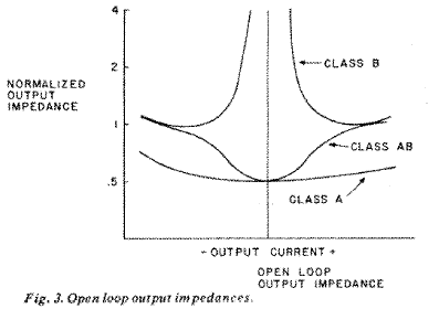
DESIGN ANALYSIS
The conceptual schematic for the amplifier is given in fig. 5, where you can see the rather conventional NPN differential front end which drives a PNP voltage gain transistor. Both parts of the circuit are biased with the constant current sources as shown, and the signal from the collector of the PNP is followed by the Darlington class A output stage whose idle current is controlled by the bias circuit. 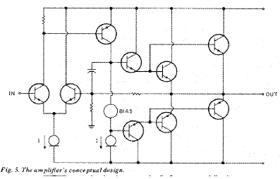
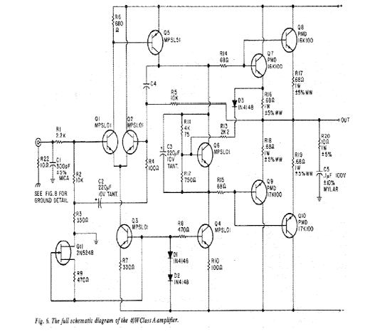
Breaking down the schematic of the actual unit of Fig. 6, we start with C1 forming an input rolloff filter in conjunction with the typical 600 Ohm to 1k Ohm source impedance. Lower frequency rolloffs can be achieved using higher capacitance values and higher source resistance values. The transistors Q1 and Q2 form the traditional differential pair but there are some twists added to the feedback and input networks. The feedback circuit formed by R3 R4 R5 C2 C4 is used to bootstrap the input impedance to a nominal value of 40k Ohms while providing a low impedance path for the input bias currents. This results in a high input impedance with low offset voltage. The capacitor C4 creates a high frequency input to the negative feedback circuit which rolls off the high frequency gain of the amplifier.
C4 frequency compensates the amplifier by creating internal feedback which allows the front end of the amplifier to work at satisfying the high frequency loop requirements by itself, ignoring the phase effects of the output stage and providing a high degree of stability for the system. As a form of feedforward technique, it does not impair the slew capabilities as lag compensation would, and comes into play at around 200kHz.
Parts List (each channel)
-
R1
-
2k2 , all resistors RN55D metal film 1% 1/4W
-
R2
-
10k
-
R3
-
330 ohms
-
R4
-
100 ohms
-
R5
-
10k
-
R6
-
680 ohms
-
R7
-
330 ohms
-
R8, 9
-
470 ohms
-
R10
-
100 ohms
-
R11
-
4k75
-
R12
-
750 ohms
-
R13
-
2k2
-
R14, 15
-
68 ohms
-
R16-19
-
0.68 ohms, 1W, 5% wirewound
-
R20
-
10 ohms, 1W, 5% Carbon comp.
-
R22
-
10 ohms
-
C1
-
300pF, 50V, 5% silver mica
-
C2,3
-
220uF, 10 V tantalum
-
C4
-
40pF, 5%, 500V silver mica
-
C5
-
0.1uF, 100V, mylar
-
Q1-4
-
MPSL 01 Motorola
-
Q5
-
MPSL 51 Motorola
-
Q6
-
MPSL 01 Motorola
-
Q7,8
-
PMD16K100 Lambda
-
Q9,10
-
PMD17K100 Lambda
-
D 1-3
-
1N4148 diode
-
Q11
-
2N5248 FET
-
Da,b
-
25A 100piv bridge
-
Ca-d
-
Capacitors, 35V, Computer grade
-
Ce,f
-
0.01uF, 1500V
-
S1
-
SPST switch, 10A
-
F1
-
10A, fast-blo
-
F2-4
-
3A, fast-blo
-
T1
-
Signal 88-8, Pri: 118V, Sec: Two 44V, CT, 8A. Alternate: 2 Transformers with 44V, CT, 6A
-
Heat sinks
-
(two per channel) Thermalloy #6560, 6590, 6660, 6690, or equiv.
DAMPING, CURRENT, OUTPUT
Fig. 7 plots the output damping factor of the amplifier vs. 8 Ohms {disregarding the impedance of the output fuse) and shows the effects of the open loop rolloff with the lead compensation versus the same capacitor used to lag Q5. Fig. 7 also shows the high, wide-band damping factor, which serves particularly well into low impedance, especially reactive loads.
We see also in Fig. 6 the two current sources formed by Q3 R7 and Q4 R10. They are driven by the voltage source D1 D2 which is a reference voltage diode pair which produces 1.3V when forward biased by the 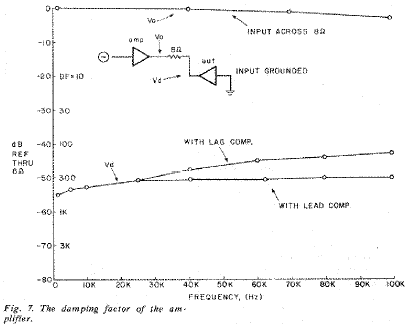 and what does creep through is removed by C3. Thus the bias circuit watches DC bias and ignores the signal.
Fig. 8a and Fig. 8b show the integration of the two amplifier channels into the overall schematic. Here we see the power supply, which in this case requires a 44V, center tapped 6A secondary winding for each channel. While two such transformers would do the task, a Signal 88-8 will do an excellent job as it has two independent sets of secondaries rated at 8A each.
Fig. 8b is also intended to show the preferred method of grounding the various. components in the system, and unless otherwise specified, every ground in the system should return as shown to only one point on the ground bus bar on the power supply capacitors. At the input terminals, you will note that the ground of the connector is not attached to the chassis, but is connected via a 10 Ohm resistor to the chassis at that point. 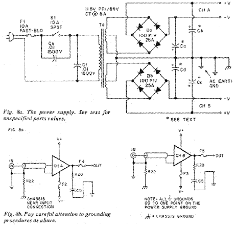
POWER PARTICULARS
The diode bridges will require some degree of heat sinking, which is easily provided by a metal chassis. The heat sinks of the amplifier and any other large metal parts must be grounded to the chassis, which in turn is connected to the ground point. The values for power supply capacitance can be realistically determined by a consideration of the numerical value of W C R where W is the line frequency (377 rad/sec), C is the power supply capacitance, and R is the load resistance.
For this amplifier, the design load is 8 Ohms (although it will easily drive 4 Ohms) at full power. An WCR value of 10 yields about 10 per cent ripple (pk.-pk. ) and a value of 100 has about two percent. Below 10, the power supply will have serious problems and values of about 100 will
current following through the current source FET Q11. This 1.3V at the base of Q3 results in a .6V drop across R7, giving the current source a value of 2mA. Q4 thus operates at 6mA (.6V)/(100 Ohm) and has the addition of R8, which prevents the reference voltage from collapsing when Q4 saturates during a negative clip, improving the recovery time.
Q11 and R8 serve to feed current to the diodes D1 D2 which provide the voltage reference for the current sources. Q11 and R8 form a current source themselves, and used instead of a resistor to bias the diodes, they provide a higher power supply rejection for the negative half of the circuit. This lowers ripple voltage noise and distortion by about 20dB.
Q7-10 are special complementary Darlington transistors, chosen especially for their rugged safe operating area and the 25 Ohm value of their internal driver's emitter resistor. These cannot be adjusted by the user and most manufacturers use about 100 Ohms in this spot, which results in far less bias on the driver transistor.
EASY BIAS
The bias network of Q6 D3 and R12 R13 serves to control the idling current of the output stage. It starts out as a conventional Vbe multiplier consisting of R11-12 and Q6, where the voltage developed across Q6 is
(.7V) x (R12+ R11)/ R12
The addition of D3 and R13 provide feedback, treating the base of the transistor as the (-) input of a summing amplifier. Inasmuch as the differential voltage between the emitters of Q7 and Q6 is relatively constant in this class A amplifier, the bias circuit rejects the AC signal,achieve diminishing performance returns. The minimum value then, for each of the four power supply capacitors should be about 3,000uF and the maximum about 30,00OuF. Capacitances above this value may cause diode bridge failure due to turn-on surges and are not recommended.
CONSTRUCTIONAL DETAILS
Fig. 9 is the full sized etched circuit board pattern for the amplifier end fig. 10 shows the location of the board mounted components and connections to the output stage. When installing the plastic transistors on the board, double check their orientation and install them with the leads left as long as possible so that heat will not easily travel up the leads being soldered into the board. [Heat sinks attached to the leads while soldering is also a good idea. -Ed.]
Fig. 9 is the full sized etched circuit board pattern for the amplifier end fig. 10 shows the location of the board mounted components and connections to the output stage. When installing the plastic transistors on the board, double check their orientation and install them with the leads left as long as possible so that heat will not easily travel up the leads being soldered into the board. [Heat sinks attached to the leads while soldering is also a good idea. -Ed.]
Fig. 10 also details the set of connections from the board to the input,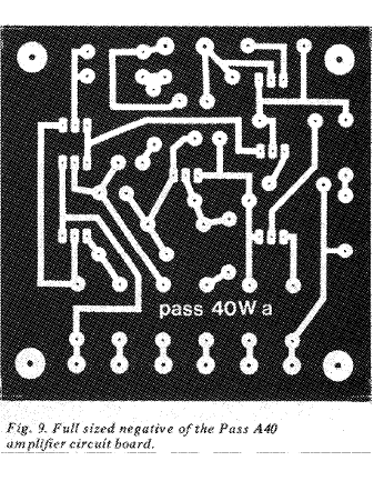
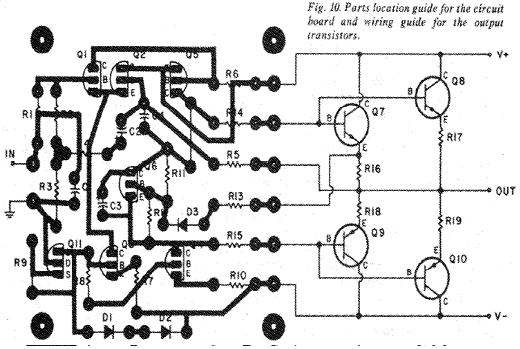
output, and output stage. Wire lead lengths should be kept short and the input signal cable should be kept away from the power supply and output cables. After the output transistors are mounted on the heat sinks using mica insulators, silicone grease, and the appropriate hardware,you may want to test for a possible short between the case of thetransistor and the heat sink.
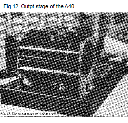
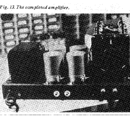
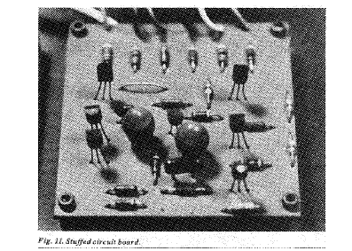
Fig. 11 is a photograph of the completed circuit board. Fig. 12 is a photograph of the output stage. The finished amplifier is shown in figs. 13 and 14.
FINAL TESTS
Needless to say, once the amplifier is completed, you should stop and recheck all steps. When you are certain no errors have been made, insert temporary 2A fast-blow fuses in F2 and F3 and 1A fast-blow fuses in F4 and F5. Turn the amp on without a source or load. If it doesn't blow the F2 and F3 fuses, you're half way home. If possible you should use a variable line auto transformer to slowly raise the AC line voltage. At this point, you may want to verify various quiescent voltages in the circuit. The output should be at 0V, the power supply should be about plus and minus 32V. The voltage across D1 and D2 should be 1.3V; across R7 and R10: about .6V; and across R6 approximately .65V.
After the amplifier has warmed up, the voltage between the emitters of Q7 and Q9 should be approximately one Volt. If you have used substitute or off- tolerance components, the bias will have to be adjusted by the value of R11.
If F2 and F3 blow upon sumon, try shorting the bases of Q7,8 to the bases of Q9, 10. If this cures the fuse blowing, check for .6V across R10 and if that value is correct, replace Q6 and possibly D3, R11, 12, &. 13.
If shorting the bases of the. output transistors does not doit, it may be that one of the output transistors is blown, which will exhibit itself as a measurable short or a 25 Ohm value between the collector and the emitter of the transistor.
If the amplifier can be fumed on without blowing F2,3 the output should be immediately checked for offset voltage with a voltmeter, and should have offset in the millivolt range.
For those of you who don't possess a voltmeter, the output may be tested for offset by installing a 470 Ohm, 1W resistor across each set of output terminals and turning on the amplifier. A heated resistor will indicate severe offset. If the amplifier can be operated without warming the resistor, however, it is unlikely to have offset voltage. Be careful not to bum yourself when you touch the case of the resistor.
If there is no offset voltage, and if the amplifier can be operated for an hour without blowing fuses, it is probably safe to connect the amplifier to a hi-fi system. If it works at low audio levels, turn the system off by unplugging the line cord, install the 3A fuses in the F4 and F5 and the F2 and F3 spots, and turn the system back on.
Proper ventilation will be important to the reliable operation of the amplifier, and as a good rule of thumb, the heat sinks will be doing an
adequate job if their heat is not painfully hot to touch.
HOW'S THE PERFORMANCE:
The following performance curves were obtained from a channel which used no matched or selected transistors. The tests were conducted at a power supply voltage of plus and minus 32V with 10,000uF power supply capacitors and a bias current of 1.5A.
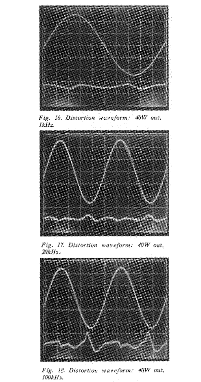
Fig. 15 shows the distortion curves versus power and frequency into an 8 Ohm load. The harmonics are primarily 2nd and 3rd order and the performance remains virtually identical for any percentage of reactance in the load including fully capacitive (example: 1uF at 20kHz}. You will note that the distortion remains low out to 100kHz, decreasing monotonically below these levels and is typically less than .01 for most of the audio signal range. Fig. 16 shows the distortion waveform of the amplifier at full power at 1kHz. 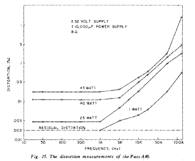
The ripple noise level is less than 1mV for the 10,00OuF capacitors, the typical offset voltage is 20mV, and the nominal input impedance is 40k Ohms. The damping factor of the amplifier is determined essentially by the output fuse, for a value of about 100, which remains fairly constant across the audio band because of the wide open- loop bandwidth and the lack of an output coil. The damping factor without a fuse is seen in Fig. 7, which is approximately 300.
Nearly all available solid state amplifiers use a coil/resistor in series with the load to enhance their stability. These typically reduce the damping factor, however to 10 or 20 at 20kHz, having a large sonic effect into purely resistive and especially capacitive loads.
DISTORTION DEDUCTIONS
The amplifier performs well under sinusoidal testing, and the reader may well wonder how this correlates to testing under transient conditions. While traditional testing procedures have not impressed most audiophiles for their exactness in a description of sonic performance, this is not the fault of the test procedure, but our interpretation of the data. The wealth of information received from the distortion waveform of 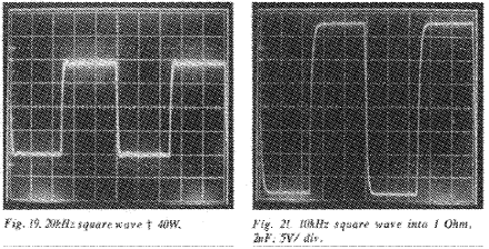 The slew rate at which slew induced distortion occurs is less than the maximum slew rate, but pinpoints the slew at which the distortion is observable. Fig. 17 shows the distortion waveform of the amplifier at full power of 20kHz (3V/us), and Fig. 18 shows the slew induced distortion which occurs at 15V/u s in a full power 100Hz wave. In this amplifier, slew induced distortion shows up at slightly less than the maximum slew, yet there are amplifiers with higher slew rates which exhibit this distortion at slew as low as 1/10 of their maximum. Much of the difference is due to simple class A circuitry. We find that the crossover notch of the output stage of many AB amplifiers aggravates the situation inasmuch as the point of maximum slew often occurs at the point where the output transistors are going through their turning on and off gyrations.
Fig. 19 shows a 20kHz square wave at 40W into 8 Ohms. Reading the ads for amplifiers rated at 100V/us, it is easy to lose one's perspective on the subject of slew rate. We have too little discussion of just what kind of slew rates are found in real hi-fi systems. To gain such a perspective, I constructed the setup of Fig. 20 where a 100W mplifier capable of 30V/us into a load has an RC differentiating network on its output. The network, consisting of a .1uF capacitor and 1 Ohm resistor, has a 100mV/(Vus) output characteristic and this is fed to a storage scope.
Simultaneously, I fed the output of the amplifier into a spectrum analyzer which peak detected the spectrum from 0-100kHz. I want through a number of cartridges and many recordings looking for the signal source that would produce the highest frequency content. Ultimately I used the Panasonic 451EPC strain gauge (with my own preamp/power source)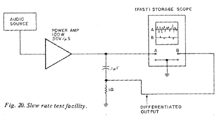
 an amplifier certainly should not be processed into a single number as it reveals much about "transient" performance.
Remember, an amplifier does not have any particular memory, and does not differentiate between a sinusoidal or a pulsed waveform - it is merely going where it is sent. "Steady state" distortion, or distortion at lower frequencies, reflects how accurately the voltage is placed, and transient distortion reflects how rapidly it can be placed.
For this reason, sinusoidal testing can reveal those distortions caused by high slew operation inasmuch as a distinct instantaneous tearing of the sine wave at some peak slew is observable with a notch filter. It will occur simultaneously with the peak slew, whose value (V/us) equals
(frequency)( PI )(Vpp)/1,000,000
and a Japanese audiophile recording on the RCA label "Check Up Your Sounds Vol. 1." The combination produced phenomenal high frequency power which hit -25dB (reference peaks below 20kHz) at 50kHz. If the amplifier were clipped, I measured the 30V/us recovery, but with unclipped performance, the highest measured slew was 1.5V/us.
In other recordings and with other cartridges, .5V/us peak slew was more common and was generally associated with cymbals and synthesizers but not piano or vocal material. I found this interesting as I had always imagined higher slews than I found. It certainly makes one wonder whether the value of high slew rate specifications isn't like damping factor, where
ODD LOADS
Apart from slew rate, amplifiers often encounter problems associated with reactive low impedance loads found in crossover networks or electrostatic speakers. As an example of this amplifier's capability into such loads Fig. 21 shows a 10kHz plus and minus 10V square wave into a 2uF, 1uF capacitor, showing a small amount of well damped ringing 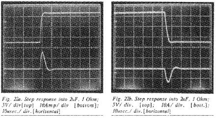 generated by the wire's inductance. To gain a greater appreciation of the demand this places on an amplifier, Figs. 22A and 22B show the response of the amplifier to step functions where an additional trace shows the amount of current output of the amplifier simultaneously with the voltage output. (Vertical: top: 10V/div; bottom: 10A/div; horizontal: 10us/div.)
From them, we see that the amplifier is delivering nearly 15 Amperes under high slew conditions without waveform breakup. The amplifier has been tested into the modified Dayton Wright XG8 MK IIIs whose impedance is .5 Ohms from 4kHz to 20kHz, without problems. It even sounds good.
In summary, here is a simple but excellent amplifier which I hope some of you will build. While a few of the parts are exotic, Old Colony Sound will be offering them as a partial kit, which should take care of the problem.
BEFORE YOU WRITE
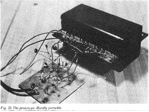
To forestall questions which inevitably arise: 1. No, you cannot easily modify the design for higher power. 2. Yes, you could decrease the bias into AB and have it work well. 3. Signal Transformer is at 500 Bayview Ave., Inwood NY 11696 (516} 239-7200 and they require cashier's checks in advance. (Their 88-8 weighs 22.8 lbs. and lists for $56.18.) 4. No parts substitutions. 5. Usually you have to get the heat sinks surplus, but I don't know where. 6. Yes, you can bridge the amplifier for mono operation. For those interested in origins, Fig. 23 is a photo of the original prototype channel. It still works quite well. However it is not very portable. Good luck.
Pass Laboratories, PO Box 219, 24449 Foresthill Rd, Foresthill, CA 95603.