Zen Amplifier Revisited
Nelson Pass
Introduction
I must say that I have been very gratified by the response to the Zen amplifier from the last issue of TM. Since writing the article I have had an opportunity?to build another 25 copies of the amplifier, listen to it on a larger variety of loudspeakers, absorb criticism from the readership, and generally meditate on the project.
Areas of criticism of the design all relate to the objective, measurable performance, but in addressing them, I found that the subjective performance improved with the measurements. All of the changes are performed without altering the original topology of the project amplifier.
Noise
The most objectionable flaw I found was the noise, specifically about 5 mV of hum that appeared at the output, which made it sound more like a tube single?ended amp. This was easily cured by cleaning up the
supply, which I approached from two directions. First I ran the amplifier from a regulated supply, and I can report that it takes care of the problem perfectly well.
Second, I created a pi filter in the existing supply using an additional 10,000 uF of supply capacitance and a 1 or 2 milliHenry air core coil separating them. This circuit is shown in the power supply portion of Fig 1. I bought the coils from MCM. The result was a reduction of the hum by about 26 dB, which made it generally inaudible.
I found that I preferred the sound of the pi filter over the regulated supply, although I can't imagine why. In either case, the amplifier sounded quite a bit better than with the original supply, not only because you cannot hear the hum, but also because ripple does not show up when over?driving the amplifier, making the clip less audible.
Capacitors
Several people wrote wanting to know how to eliminate the capacitors from the circuit. This is not a practical thing to do, but there are
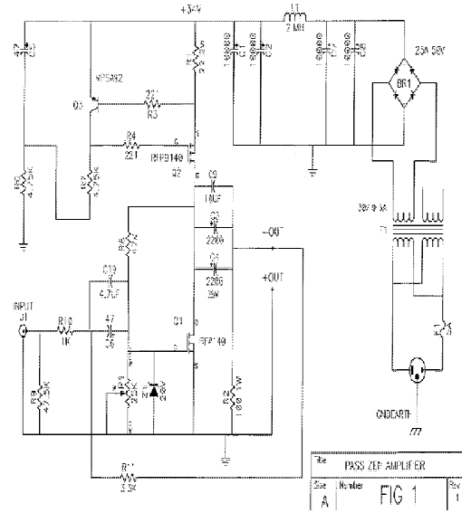
improvements we can make in this area also. First, it is perfectly acceptable to bypass the electrolytic capacitors with higher quality film types, as shown in Fig 1.
Second, it is easy to restructure the feedback loop of the amplifier so as to enclose both the input and output capacitors in the loop, reducing their distortions by the amount of feedback employed. This is shown in Fig 1, where the values of R8 and P1 have been increased, and two new resistors, R10 and R11 form a separate feedback loop outside the capacitors.
R8 and P1 are still necessary for the purpose of setting the DC bias point of the system, but by making their impedance values high compare to R10 and R11, we allow R10 and R11 1 to dominate the performance.
Enclosing the DC input and output of the circuit with the R10 and R11 feedback loop also allows us to adjust the gain of the circuit independently of the DC bias adjustment, which comes in handy later.
Distortion
Probably the most criticized aspect of the performance from people who have not built and listened to the amplifier, was the distortion performance as documented in the article. Some people have become confused as to the source of the distortion, blaming single?ended operation for the THD figures, when in fact the culprit is the simple nature of the single gain stage.
There are certainly things we can do to improve the distortion figures of the amplifier, both in terms of distortion vs. level and vs. frequency.
First, the choice of Mosfet will have a significant influence on the distortion figures. I have built the circuit with IRF240, IRF140, and IRF040. These devices are very similar, but have been doped somewhat differently for the purpose of voltage ratings. The higher the voltage, the lower the transconductance, and the higher the distortion in the circuit. The original curves reflected the 040, and subsequent use of a 140 gave harmonic distortion figures about 50% higher, and the 240 about 100% higher. For example, at 1 watt at 1 KHz, the 040 gave about .6%, the 140 gave about .9%, and the 240 about 1.2% harmonic distortion.
Outro
All this presumes that your source can come up with the 3 volts to drive these lower input impedances. It is acceptable to scale R10 and R11 up or down, or to change their ratio and the gain, in order to best accommodate the capabilities of the source. Feel free to experiment!
I have as an upcoming project a preamplifier circuit suitable for driving this input network, as well as plans for a more powerful version of the Zen amp.
In the meantime, thank you for all your responses, particularly the complaints, diatribes, and screeds.
Miscellaneous: Fig 3a and Fig 4 artwork in the original article are flipped, and an MPSA92 transistor in the part list is incorrectly identified as an NPN transistor.
White papers and product literature:
Pass Labs
PO Box 219
24449 Foresthill Rd.
Foresthill, CA 95631
fax 530 367 2193
copyright 1994 Nelson Pass
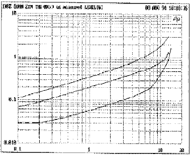
Second, the amount of bias on the Mosfet will make an appreciable difference: Fig 2 shows an IRF140 biased at 2 amps (top curve) and 3 amps (middle curve), and the distortion has dropped by half. The increase in current is accomplished by reducing R1 from .33 ohms to .22 ohms. The dissipation in the power transistors goes up from about 30 watts each to 45 watts, and you want to increase the heat sinking appropriately if you make this change. Also, you should be prepared for a somewhat shorter life span of the amplifier.
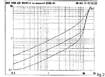
Third, you can adjust the values of R10 and R11 to reduce the gain of the amplifier, increasing the feedback. Fig 3 shows an IRF140 operated with 2 amp bias (top curve) and 3 amp bias (middle curve) with R10 at 1 Kohm and R11 at 3.3 Kohm. The gain figure here is 8.5 dB, and it takes 3 volts to drive the amplifier.
Fourth, you can parallel the channels at the input and outputs to obtain still lower distortion figures. The bottom curves of Fig 2 and Fig 3 were obtained by parallel the channels with 3 amp bias.
In the case of the bottom curve of Fig 3, we are now obtaining distortion figures 20 dB down from the original circuit, giving the Zen amplifier a cloak of objective respectability. These curves are for the IRF140, and somewhat better measurements are obtained by using an 040. The choice of P channel device is much less important, as it is simply configured as a constant current source.
Distortion versus frequency is essentially a function of the impedance of the input/feedback network. Since the network has to charge the nonlinear capacitance of the Mosfet, lower impedances will give better figures. Since the revised network of Fig 1 has about 1/5 the impedance, the knee of increased distortion versus frequency is moved up by a factor of 5 or so.
Running greater current and parallel channels improves the damping factor in the same kind of proportion. In the test case, the damping factor went from about 8 to about 30.