Zen Variations 4
Nelson Pass
Introduction
The Penultimate Zen is the sum of several incremental improvements to the original Zen amplifier of 1994. Eight years just flies by, doesn’t it? These improvements are contained in parts 2 through 4 of the Zen Variations, and is likely the last version of this amp, although by no means the end of the variations on the theme of single stage amplification.
In part 2 we developed an improved active current source load for the single gain device which is at the heart of the amplifier. Originally designed for the Aleph amplifier series, this current source doubles the output current and significantly lowers the distortion of the circuit over the original constant current source. As the original Zen amplifier is limited in both power and fidelity, this is a welcome improvement.
The original Zen amp is also limited in its rejection of power supply noise, and benefits from having a quiet, stable power supply. In part 3 we discussed some possibilities for power supply regulation for this and other Zen amplifiers.
The final shortcoming we will address in the Penultimate Zen is the low input impedance. Depending on the version and the desired gain and distortion figures, the original Zen amp has an
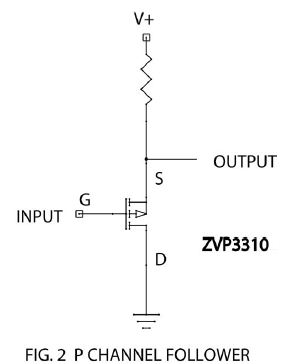
There is another, more clever way to accomplish this follower, as seen in Figure 2. Here we use a P channel Mosfet with the Drain connected to ground and the Source biased up by a current source, in this case just a resistor. There are several advantages to this approach:
First, the input can be direct coupled, as it operates at ground potential, eliminating the input capacitor and bias circuit.
Second, it is self-adjusting in the sense that the Source will operate at +Vgs where Vgs is the Gate to Source voltage for the Mosfet, or about 3.5 volts. The amount of current supplied by the resistor is not critical, and can be quite high if desired, as the Mosfet will only dissipate that current times the Vgs value. For the ZVP3310 we will be using, you could run it as high as 50 mA, which is a lot.
Third, the P channel non-linearity will tend to operate in opposition to the N channel distortion of the gain Mosfet, giving some distortion reduction due to cancellation. You can adjust this cancellation a bit by adjusting the bias current and loading of the P channel device.
Fourth, because the input system is at virtual ground, we can swing all the drive current we want without being concerned about the voltages across the input device, since it will be held very close to the constant Vgs of the P channel input. No Miller effect, hardly any gain or capacitance modulation, better performance.
Talk amongst yourselves. I’ll give you a topic: Is this still considered a single gain stage circuit? If a Differential pair or Darlington or a Cascode is considered single-stage would this be also?
input impedance that varies from 600 ohms to a couple thousand ohms. For many audio sources, this input impedance is simply too low to give optimal performance. The ideal input impedance would be something up around 47 K ohms.
We will address this fault here and now, and then go on to present a final circuit with a nice finished printed circuit board design.
Upping the Input Impedance
The issue of increasing the input impedance of the Zen amp is a delicate one. There is no way around the need to add circuitry to accomplish this, but in the spirit of the Zen amp, we wish to do it minimally.
The input junction of the gain Mosfet of the amplifier is operated at virtual ground, so that previous Zen amps have an input impedance which is the value of the input resistor between the input connector and the Gate of the Mosfet. You could simply increase the values of the input and feedback resistor, but then you bump into the non-ideal nature of the Mosfet.
The Gate of the Mosfet has essentially an infinite input impedance at DC, but offers capacitance between the Gate and Source and the Gate and Drain pins. The amount of the capacitance is not so great and by itself does not impose serious limits on the resistor values. The problem is that this capacitance varies under differing voltage and current conditions, and is thus non-linear in character, creating distortion at higher frequencies. You can see this effect clearly on the distortion versus frequency curves of the previous Zen amplifiers, where somewhere above the midrange the harmonic distortion begins increasing with frequency. The higher the resistance at the input, the earlier this effect starts.
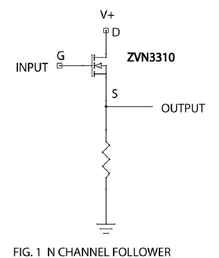
To have a high input impedance while maintaining low distortion at high frequencies, the amp needs a buffer. The most obvious approach is to use an input follower as seen in Figure 1. Here a small N channel Mosfet is biased up to served as a Source follower, presenting a very high input impedance, and a fairly low output impedance while following the input voltage. Since we use a small Mosfet for this purpose, the input capacitance is tiny enough to not have a significant effect at audio frequencies.
The Circuit
Figure 3 shows the circuit of Figure 2 incorporated into the Zen Amp with the regulated power supply. Q4 is the added buffer transistor, and it is biased by R13. R9 and C7 filter the voltage provided to R13. The feedback loop of R2 and R3 which previously connected to the Gate of Q1 are now connected to the Gate of Q4 and have values two orders of magnitude higher, giving the amp an input impedance of 47 K ohms.
This circuit was designed to idle at 2 amps, which is more than it actually needs to achieve the 25 watt into 8 ohm figure desired. R0 and R1 together form a .33 ohm resistor, and if you leave R1 out, the bias figure drops to 1.3 amps. With both R0 and R1 and a 50 Volt rail, the amplifier will dissipate 100 watts, and with R1 removed, the circuit dissipates 67 watts at idle.
Depending on your heat sinking and power needs, you can include R1 or not. If you are planning on driving 4 ohms, you will definitely want it. If you leave R1 off, you also should change the value of R16 from 1.5 K ohm to 1.0 K ohm.
As with all the Zen amps, very few of the component values are critical, in fact none of them are, so if you have resistors and capacitors which come close to these values, feel free to use them.
As discussed previously, many substitutions will work for the transistors. Q2 and Q5 can be chosen from a wide array of IRF type N channel devices as long as they have the power and current rating to do the job, which would be around 150 watts and 10+ amps. They do not have very much influence on the sound compared to Q1 and Q4.
In the case of Q1, the IRFP044 is the preferred part, but you can get almost as good performance from the IRFP140 and 240 parts, and pretty much anything else that is similar in character.
In the case of Q4, the Zetex ZVP3310 performed the best among the parts tried. The IRF9510, 9610, and similar parts worked, but have higher capacitance, and thus higher distortion at the top end with these input impedances. This can be improved by lowering the values of R2 and R3. If you can accept a 10K input impedance, you could consider using these alternate P channel Mosfets.
While we’re talking about the input, note that the input of this amplifier is not protected against high voltage transients. Input voltages in excess of 20 volts will have some chance of damaging the input Mosfet Q4. If this occurs, it should not create damage to
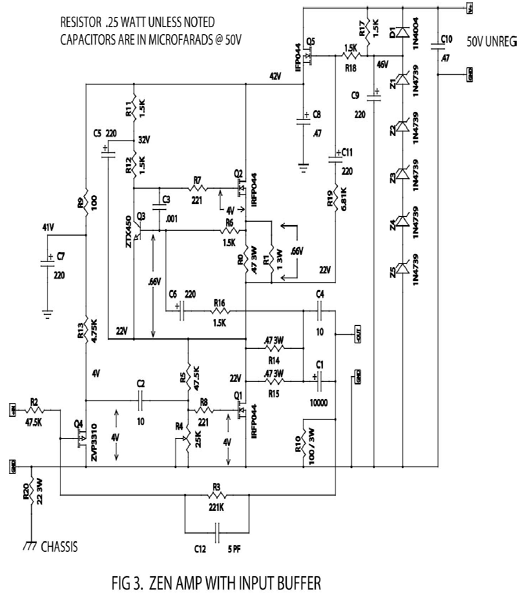
other parts, so if you plan on being careless when connecting the amp up, keep a couple of spare ZVP3310’s laying around.
Q3 works well with the Zetex ZTX450 NPN transistor, but we note that any decent NPN signal device will work here, as we are primarily using it for the .66 volt junction voltage to control the current through Q2. Like most of the parts here, it was chosen because it is available through Digikey.
C4 is simply a bypass capacitor for C1. It may be omitted altogether or replaced with your favorite bypass part. C2 can be electrolytic or film (film being preferred) but should be at least 10 uF to avoid low frequency rolloff. If C2 is an electrolytic type, the polarity will not usually be important as the DC values on either side are approximately the same. If you find that they are not, you will know where to point the + side, won’t you?
For more commentary on the main audio circuit, refer to Zen Variations part 2.
C8 and C10 are simply high frequency bypass capacitors.
Usually the circuit will work fine without them, but they provide a nice margin for stability. Similarly with C12, which trims the high frequency response so as to avoid peaking at high frequencies. Digikey doesn’t have 5 pF caps anymore, but I have listed 10 pF parts in the parts list. You can buy 2 and put them in series to form a 5 pF capacitor. Alternatively, you can twist two fine insulated wires (like those used in wire-wrap construction) together at a length of about 1.5 inches and get about 5 pF. This technique has the advantage that you can start out too long and trim it with a pair of scissors while watching the square wave of the amplifier.
Z1 through Z5 are 9.1 Volt Zener diodes which create a 45.5 Volt reference for the regulator Q5. You can adjust these to different voltages or bypass any of them if you find yourself using a different rail voltage. You can leave them out altogether, in which case the regulated supply will be about 4 volts less than the unregulated supply, but with the AC ripple removed. This works just fine in practice, and is usually referred to as a capacitance multiplier. For more information on the other parts in the supply regulator, refer to Zen Variations part 3.
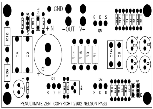
Figure 4 shows the printed circuit board for this project. It measures about 6.5 X 3 inches and holds the circuitry shown in Figure 3. The board is available for sale from www.passdiy.com and you can also download the Gerber files to get your own made.
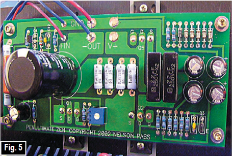
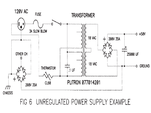
Figure 5 shows the board all stuffed up. This board does not include the components for an unregulated 50 volt supply, but Figure 6 shows a typical circuit for one channel and the grounding layout for a stereo amplifier. The transformers are Plitron 077014201, with two 18 V secondary windings and a 300 VA wattage rating. While two transformers are recommended for two channels, we did build an amplifier up using only one. It
worked well enough, but ran hot and mechanically buzzed a bit at 200 watt draw. Note in Figure 6 that we have chosen to isolate the two channels through a rectifier bridge to ground, with each channel’s ground appearing on one of the AC legs of the bridge. If you use a single transformer supply for two channels, tie both of their grounds together and to both AC legs of the bridge.
If you construct the amplifier with two separate transformers and decide to operate the amplifier balanced or bridged, be certain to tie the ground speaker outputs together with a heavy piece of wire to provide a good low impedance ground connection between both channels, otherwise speaker current will attempt to flow through the input ground cables.
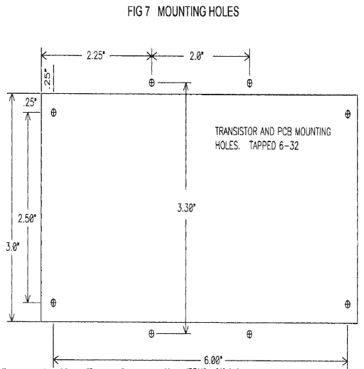
Figure 7 shows the mounting hole dimensions for the board and power transistors. These holes are tapped 6-32 onto a flat surface of a heat sink. The power transistors must be insulated from the heat sink using thermal insulators, either silicone pads or mica and thermal grease. Use a washer between the head of the screw and the case of the transistor to spread the force across the package, and don’t tighten them very tight. The ground on each board connects to the heat sink through R20, providing a resistive connection to the chassis.
The heat sinks will have to dissipate up to 100 watts per channel, and need to do so with a temperature rise of about 30 degrees Centigrade, which gives them a rating of about .3 deg C. / watt. If you use smaller sinks, then a lesser bias (no R1) and/or fan cooling will be necessary.
If you manage to cool the amplifier very well, you can consider whether you can get more power out of it. I would say the practical limit to this will be Q1, which is run at about 44 watts with the 2 amp bias. Personally, I hesitate to operate this device at greater than 50 watts, but you can crank the supply voltage and bias up higher if you want. With the IRFP044 I would not exceed 50 volts on the regulated supply. If you want to try higher, I suggest the
IRF140 or 240 devices.
More bias is easily provided by replacing R1 with .47 ohms, which will give you 2.8 amps, enough to probably get 50 watts into 4 ohms and 100 watts balanced into 8 ohms. Beyond this, you can expect some excitement. If you do replace R1 with .47 ohms, I suggest R16 at 2 K ohms or so.
REFERENCE
DESCRIPTION
DIGIKEY PART #
Q1, Q2, Q5
IRFP044 N CHANNEL POWER MOSFET
IRFP044N-ND
Q3
IZETEX NPN ZTX450
ZTX450-ND
Q4
ZETEX ZVP3310 P CHANNEL MOSFET
ZVP3310A-ND
D1
1N4004 DIODE
1N4004GICT-ND
Z1 - Z5
1N4739 9.1V ZENER DIODE
1N4739ADICT-ND
C1
10,000 uf @ 50 V ELECTROLYTIC
P6939-ND
C2, C4
10 uF POLYESTER FILM
EF1106-ND
C5, C6, C7,C9, C11
220 uF @ 50V ELECTROLYTIC
P1246-ND
C8, C10
.47 uF POLYESTER FILM
E1474-ND
C12
5 pF FILM
399-1806-1-ND (2 IN SERIES)
R0, R14, R15
.47 OHM 3 WATT METAL FILM P0
.47W-3BK-ND
R1
1 OHM 3 WATT METAL FILM
P1.0W-3BK-ND
R2, R5
47.5K .25 WATT METAL FILM
47.5KXBK-ND
R3
221K .25 WATT METAL FILM
221KXBK-ND
R4
25K TRIM POTENTIOMETER
3386P-253-ND
R6, R11, R12, R16, R17, R18
1.5K .25 WATT METAL FILM
1.50KXBK-ND
R7, R8
221 .25 WATT METAL FILM
221XBK-ND
R9
100.25 WATT METAL FILM
100XBK-ND
R10
100 OHM 3 WATT METAL FILM
P100W-3BK-ND
R13
4.75K .25 WATT METAL FILM
4.75KXBK-ND
R19
6.81K .25 WATT METAL FILM
6.81KXBK-ND
R20
22 OHM 3 WATT METAL FILM
P22W-3BK-ND
Figure 8 shows the parts list. All the parts except the transformer and mechanical package can be found a Digikey ( www.digikey.com ).
The amplifier is not very susceptible to noise pickup, and you can get good results enclosing it in a wooden chassis. If you do, be certain to heat sink the rectifier bridges, which ordinarily get their heat sinking from the chassis. Placing them on the main sinks is OK.
Adjustment
Assuming that you have triple checked your assembly work, it is time to “light this candle”. Do so one channel at a time connected to unregulated V+. Wear safety glasses. Fuse the transformer at the minimum value, about 1.5 amps. Set R4 at maximum value, which is counter-clockwise. Bring the amplifier up slowly using
check the temperature of the heat every few minutes. Check for burning smells. Readjust R4 after an hour.
Performance
In addition to having the high input impedance, this circuit also measures better than the previous editions. Due to the regulated power supply, the noise is about 35 micro Volts at the output, a really excellent figure.
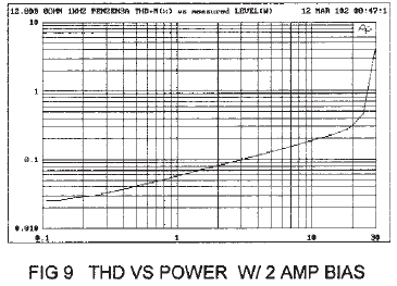
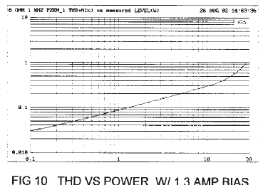
The distortion plus noise versus power into 8 ohms at 1 KHz is shown in Figure 9 with the 2 amp bias. Fig 10 shows the same curve at 1.3 amp bias with R1 removed and R16 at 1.0 K ohms.
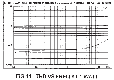
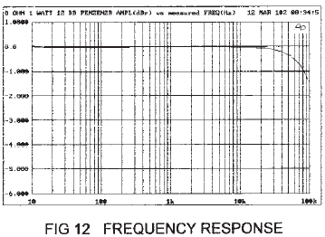
Figure 11 shows the distortion at 1 watt from 20 to 20 KHz, which is dramatically better than any earlier Zen amp. Figure 12 shows the frequency response, which is totally flat at 10 Hz, and down about 2 dB at 100 KHz.
Like just about any other amplifier, the Penultimate Zen will drive 4 ohms also, but at a higher distortion figure. If you include R1, you should get about 30 watts into 4 ohms. If you decide to run a pair of the channels balanced (or bridged) with R1 installed you can expect to see about 60 watts into 8 ohms, and the performance is very good. As documented in Zen Variations 1 and 2, the distortion tends to drop due to cancellation of the second harmonic which is the dominant distortion. This mode of operation is highly recommended if you need the most power possible into 8 ohms.
Conclusion
Sonically, this is about as good as it’s going to get for this topology, and I would match it up against an Aleph 3 without hesitation, and indeed the performance is quite similar. It’s signature is relaxed
So there we have it. The amplifier is called the Penultimate Zen because it represents how far we want to take this particular topology without getting medieval.
Thanks to Karen Douglass, Wayne Colburn, and Desmond Harrington for their help.
a Variac and watch the voltage across R0. If it does not exceed .7 volts or so, then continue to increase the Variac. Adjust R0 so that the Drain voltage of Q1 is 1⁄2 the regulated voltage plus about 2 volts.
If you get this far without problems, then check for the other voltages called out in the schematic. Readjust R4 after the amplifier has warmed up for a couple of minutes. Now do the same thing for the other channel. Watch where you stick those probes!
If the voltages all check out then you have a 95% chance that everything is proper. If not, it is time do start doing your detective work. This is best done slowly. Wait till the next day. The vast majority of problems are board stuffing and wiring errors. Look for those at length before picking up a soldering iron. Think about it twice.
When you have the bugs out, run both channels for an hour and
and very easy to listen to, although it is not a powerhouse at the bottom end. It works best with 8 ohm speakers, 90+ dB sensitivity, and not requiring a lot of control from the amplifier. In other words, a tube friendly loudspeaker.
Does it sound like a tube amp? It’s a little bit of a cross between tubes and solid state, but it has it’s own character, the result of a very simple Mosfet circuit operated pure Class A.