The PLH Amplifier
Nelson Pass
Introduction
In 1969 John Linsley-Hood wrote in Wireless World:
During the past few years a number of excellent designs have been published for domestic audio amplifiers. However, some of these designs are now rendered obsolescent by changes in the availability of components, and others are intended to provide levels of power output which are in excess of the requirements of a normal living room. Also, most designs have tended to be rather complex.
In the circumstances it seemed worth while to consider just how simple a design could be made which would give adequate output power together with a standard of performance which was beyond reproach, and this study has resulted in the present design.
He then described a Class A power amplifier using three gain stages of Bipolar transistors in a topology which continues to be admired for its elegant simplicity and sound quality.
The centerpiece of this design is the middle stage, an NPN transistor used as a phase splitter, simultaneously driving the positive half of the output stage and the negative half with symmetric signals of opposite phase.
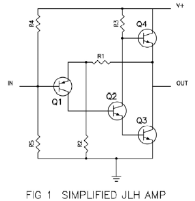
Figure 1 shows a simplified version of the JLH topology. Signal input appears at the Base of Q1, and is amplified and inverted to drive the Base of Q2. Q2 acts as a gain device and also a signal splitter, driving both Q3 and Q4 simultaneously, but out of phase with each other. Q3 and Q4 form the output transistors, Q3 operating as a Common Emitter gain device, contributing current and voltage gain, and Q4 operating as a Common Collector device contributing only current gain. The resistors provide bias for the system, and R1 and R2 feed the output of the amplifier in a loop back to the emitter of Q1.
Q2 is the heart of the design, and in my opinion, it is the elegant economy with which it performs the complementary gain to drive the output devices that gives the circuit its classic beauty.
The JLH was designed at a time when “the tube era was in decline” and the new generation of designers were pulling out all the stops to create big science amplifiers - pure voltage sources with high power and infinitesimal distortion – complex circuits with lots of feedback.
36 years and a little progress later, we can perhaps appreciate the simple charm of the JLH topology as an exercise in minimalism, but if you haven’t listened to one, you might be very surprised by the quality of sound, which is extraordinarily good within it’s power limitations. If you have efficient speakers and you like to listen to two-channel sound at reasonable levels, the JLH is still in the top rank.
The amplifier has reasonable specifications; nothing special that isn’t wildly exceeded by a $3 chip, but it produces real music. Its flaws are not irritating and it does a wonderful job wringing more music out of modern recordings and even MP3’s. I can’t think of another transistor design from that era that works as well.
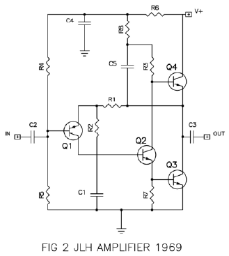
Figure 2 shows the circuit rendered more completely, but for more extensive documentation on the versions of the JLH amplifier, I recommend The Class A Amplifier Site:
www.tcaas.btinternet.co.uk
In Figure 2 additional details of setting up the DC bias for each device are shown, where capacitors are used to separate DC values from AC values. C1 separates feedback from bias current. C2 separates input signal from input DC bias voltage and C3 blocks the output DC of the amplifier from the load. C4 removes supply noise from the voltage powering the front end of the amplifier, and C5 forms a “bootstrap” circuit, making resistors R5 and R6 behave more like a constant current source at audio frequencies.
The original JLH amplifier has approximately 55 dB of open loop gain divided into 22 dB of amplifier gain and about 33 dB of feedback. As detailed in the original article, it delivered 10 watts at approximately .1% harmonic distortion or less.
The amplifier’s popular longevity speaks volumes about the quality of its sound, and this is understandable given its simplicity coupled with excellent measured performance. It has a particularly tube-like quality compared to the more complex solid-state designs of the era and since.
The distortion is largely 2nd harmonic, and is closely proportional to the output voltage. This means that .01% distortion at .1 watts becomes 1% at 10 watts, and you can draw a pretty straight line between the two points on a logarithmic graph. Such a curve is characteristic of a single-ended output topology, and there have been arguments regarding whether or not the output stage is single-ended Class A, push-pull Class A or a mixture of both. We will be having some fun with that later.
One flaw in the original JLH design was that its bias current, that idling current which flows through the parts of the circuit, had some dependency on the power supply voltage, resulting in altered performance for different AC line voltages. Power supply regulation solves this problem neatly, but there were other ways this was addressed in later versions of the circuit.
Newer JLH Circuits
John Linsley-Hood published an update to the amplifier in 1996 that addressed bias stability issues, parts substitutions, and provided a version that had a direct-coupled output, eliminating the output capacitor. At the same time, it was in many ways the same amplifier, the measured performance being very similar.
The JLH circuit continues to be interesting to the audiophile community and has been the subject of several updates. Figures 3 and 4 show simplified schematics of later generations of JLH amplifiers.
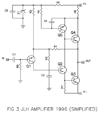
Figure 3 shows a simplified schematic of the 1996 version published by John Linsley-Hood that fixes the bias stability issue with the addition of Z1 and the Q5 portion of the circuit. This version also direct coupled the output of the amplifier, using dual supply rails.
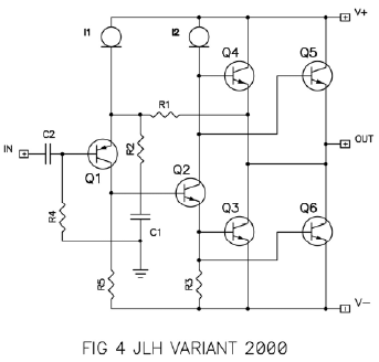
In 2000 someone else produced the circuit seen in Figure 4, where constant current sources are used to bias the first two gain stages, giving good power supply rejection to the circuit. This version also doubled up on the number of output devices. You will notice that Fig 1 – 4 have their feedback loop addressing the Emitter of the feedback transistor. Nowadays they have gotten fancy and call it “current feedback”.
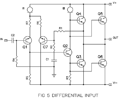
Just for your entertainment, I cobbled together the circuit of Figure 5 shows an example with a differential input. An obvious variation, but I haven’t seen it used. You can drive this input stage with a balanced signal by lifting C1 from ground and driving it as a negative input. At 100 ohms each, R6 and R7 will give this input about the same open loop gain as the original input transistor with the 220 ohms degeneration of the original feedback impedance.
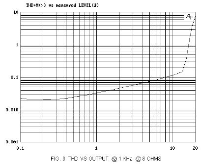
I recently measured the performance of a working copy of the circuit of Figure 4. It had 17.5 volt supply rails and was biased at about 2 amps per channel. The open loop gain is also about 55 dB into 8 ohms, and its measured performance is comparable to the original circuit.
Figure 6 shows the distortion versus output power. The bandwidth of the amplifier is –3 dB at 100 KHz, the damping factor is about 35, and the distortion versus frequency is fairly flat, rising slightly at 20 KHz.
The PLH Amplifier
One of the issues that arise from adding gain stages to amplifiers is that while they increase the open loop gain and allow more feedback correction, they themselves are the source of additional distortion. While the extra feedback can lower the distortion numbers, usually the additional circuitry is reflected in a more complex distortion character having higher order harmonics and inter-modulation components. These are generally agreed to be less musical sounding.
Michael Cunningham wrote, “Novelists must usually decide what degree of slavish accuracy would make their stories more alive, and what degree would make them less.” The amplifier designer has a similar problem to solve. It’s not hard to make an amplifier that measures well – it’s comparatively hard to please audiophiles.
My own approach is to make the signal path as simple as possible, work to lower the distortion of that basic circuit before feedback is applied, and then apply minimal (or no) feedback, largely in agreement with the comments in Linsley-Hood’s original article. The result is not always the best objective measurements, but the sound is often interesting.
The 3-stage topology of the JLH amplifier routinely uses simple Class A operation and about 33 DB negative feedback to achieve this performance, and this lured me to consider what kind of amplifier I could achieve with an even simpler circuit and less feedback. The output stage and the intermediate phase splitter cannot be dispensed with and still resemble a JLH, but you can certainly remove the input transistor.
By thumbnail calculation, the input transistor of the JLH contributes about 27 dB of voltage gain. Remove it and the open loop gain of the amplifier drops into the region of about 28 dB. If we scale back the gain of the amplifier from 22 dB to 18 dB, we end up with about 10 dB of feedback – a very minimal amount. Unfortunately only 10 dB of feedback means that the original amplifier will likely deliver something more like 1.5% distortion at 10 watts. Since such a figure is better than that seen on many single-ended Class A tube amplifiers (SET), this might be an acceptable amplifier. Actually, since the input transistor is no longer contributing to the distortion figure, we would expect the performance to be better than that, and maybe that’s the point.
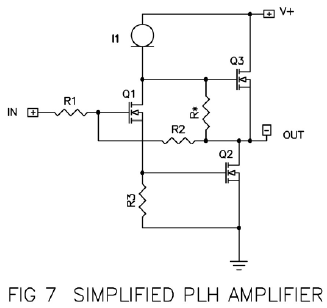
With that in mind, I stripped down the JLH to the simpler Mosfet topology shown in Figure 7, and (ahem) added my initial to the name.
I chose Mosfets for their high input impedance and because they really deliver their most linear operation in Class A mode. Since the JLH performs two phase inversions in the signal path, removing the input leaves the amplifier phase inverting, and we will be labeling the output node as “minus” and the output ground as “plus”.
The feedback path of R1 and R2 now addresses a “virtual ground” at the Gate of Q1. Q1 is biased by a current source I1, and drives the Gates of Q2 and Q3 simultaneously with voltage of opposite phase.
As a concept, you can get about 35 dB open loop gain from this circuit with the Mosfets we intend to use. You would only see it at lower frequencies however, because the Gate capacitance of the Mosfets will come into play at the higher audio frequencies.
To give a more uniform open loop gain to this circuit across the audio band, and a more interesting comparison to the original circuit, we will be choosing our values to be more similar to the original JLH without the input transistor, which means that for the circuit of Figure 7, we would be adding .47 ohm Source resistors to Q2 and Q3, and this will give us about 26 dB open loop gain.
Like the original JLH, this circuit operates between a positive voltage and ground, so you will need input and output coupling capacitors. There is no reason that it can’t be made directcoupled using dual supplies, but we will save that for another time.
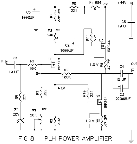
Figure 8 shows the actual circuit. As with the simplified circuit, Q1 is the input transistor and the feedback is accomplished through R1 and R2. The Source of Q1 follows the Gate input signal and drives the transistor Q3 in Common Source mode (voltage and current gain). The Drain of Q1 delivers an inverted and amplified version of the input signal to drive transistor Q3 in Common Drain mode (current gain).
The idealized current source I1 and R* of the simplified circuit is replaced by the network of P2, R4, and C2. C2 creates a “bootstrap” connection to the output that makes P2 look like a constant current source in parallel with R*, approximately the resistance between the wiper and the counter-clockwise connection of P2. P1, R6 and C5 form a filter to take out power supply noise, and adjusting P1 will set the bias current of the amplifier.
P2 will be used to set the relative gain contribution of the upper transistor Q3 versus the lower transistor Q2, but does not affect the bias current or output DC value.
Most of the resistors are ¼ watt types, but I recommend a 3 watt value for R4 and R8 and R9. The capacitors are all rated at 50 volts. None of the values needs tight tolerance. P2 is best chosen as higher wattage type. You can get by with 2 watts, but 5 watts is preferred.
I have shown nominal voltages on the schematic as guides. The circuit will work with supply voltages from 35 to 45 volts without modification using P1 and P3 potentiometers to adjust the bias current and output DC. This particular amplifier is biased at 2 amps, and the output voltage is set at 20 volts, or one-half of the 40 volt supply value.
The Mosfets used are fairly arbitrary, and in general you can substitute similar types. Since virtually all the power Mosfets are rated at least 40 volts, you are left wide latitude of choices of vertical types. Lateral Mosfets would also work with adjusted resistor values. Remember that all Mosfets are static sensitive. It is not necessary to match the Q2 and Q3. If you send me a bag of high power Jfets, I’ll supply a schematic that will work with them, too.
You will need a power supply that happily sources 35 to 45 volts at 2 amps per channel. A regulated supply is most ideal, as the bias will vary in rough proportionality to supply voltage, although we built four units without a regulated supply and they work fine. The heat sinks should be able to dissipate about 70-90 watts per channel with a rise of about 25 degrees C. You can find examples sprinkled about at www.passdiy.com and elsewhere
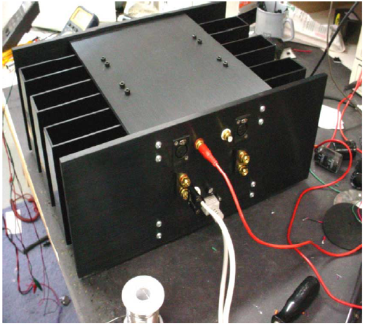
This summer, Chris and Matt Williams helped me to build the amplifiers and they all worked the more or less the same. Lucky boys, they got away with two of them. These were made from machined plates of aluminum, bolted together, with heat sinks made from square aluminum tubing and all of it anodized black. The wiring was all point-to-point on an output stage PC board. Here’s a picture:
PHOTO 1 REAR VIEW OF FINISHED AMPLIFIER
We used a transformer with a 35 volt secondary rectified into a 30,000 uF capacitor. We filtered that supply voltage through a 0.5 ohm @ 25 watt resistor to another 30,000 uF capacitor which reduced the ripple noise by about 20 dB. This powered both channels.
Remember to use good grounding – a star ground at the (-) terminal of the second capacitor is a good idea, and keep the input and grounding leads away from the power supply components, or you will pick up noise. The chassis should always be Earth grounded to the AC power plug, and the circuit ground was connected to chassis through a 5 amp power thermistor.
Adjustment
At a minimum, adjustment of the amplifier requires a DC voltmeter. I recommend the use of a Variac to slowly turn on the AC power for your initial check out. Before you apply power to the amplifier, set the value of P1 to its maximum resistance, which should set the bias at a minimum current. Set P2 and P3 at their midpoints.
I recommend firing up (unfortunate phrase, that) one channel at a time, with the other channel disconnected from the supply rail. It’s a good idea to put a 3 amp fast blow fuse in series with the positive rail of each channel, and to keep some spare fuses handy.
When power is applied, the output of the amplifier, the voltage across the Source resistors R8 and R9 should be less than 1 volt. The output DC voltage, as seen on the Drain of Q2 should be somewhere around 20 volts.
If you can bring the supply rail up to 40 volts without having the bias go above 1 volt, then adjust P3 to put the output voltage at about one-half the supply voltage (20 volts with a 40 volt rail). Now slowly decrease the value of P1 until the Source resistor voltage approaches 1 volt.
As the channel warms up, adjust P1 and P3 in small steps so that the output is at 20 volts and the voltage one of the Source resistors 1 volt. Watch the output voltage and current draw for a half hour or so, readjusting as needed as the circuit warms up. The bias will tend to drift up, but the DC output value will tend to be more constant. At the end of this procedure you should have a stable channel.
If you share two channels off a common supply, you will be taking another look at these settings later because the supply voltage will drop volt or more when both channels are connected.
Performance
The final adjusted circuit has an open loop gain of about 26 dB, a closed loop gain of 16 dB, and uses about 10 dB of negative feedback. The bandwidth is -3 dB at about 1 Hz and 100 KHz. The (unweighted) noise is about 80 uV. The input impedance is about 14 Kohms, and the output impedance is about 3 ohms (a damping factor of 2.5).
The upper and lower output devices share the same value of DC current, but as mentioned before, this circuit can be adjusted to vary the AC current contributions from each. When the values are set equal then the classic push-pull balance is achieved. By adjusting P2, you can shift this balance so that one device takes a larger share of the output.
As you turn P2 clockwise (note the “cw” on the schematic), a greater percentage of current comes from the upper device Q3, and as you turn it counter-clockwise, a greater percentage comes from the lower device Q2. Fully counter-clockwise results in the upper transistor bank functioning as a constant current source, with all the gain in the lower bank, operating as a purely single-ended Class A circuit. An 80% clockwise rotation of P2 gives about a 1:1 ratio between the devices (as the pot rotates through about 10 hours of a clock, with full clockwise as 11 PM, you would set the pot to 9 PM).
Linsley-Hood spent some time experimenting with his circuit using mismatched output devices and noted that if you don’t have equal gain, it is better to place the devices with greater gain on the bottom of the circuit. I confirmed that this was the case by adjusting the balance between the positive and negative halves of the output stage, measuring and listening to various settings.
I spent a great deal of time playing with this balance, trying to reconcile the best curves to the best sound. At low and mid-band frequencies, setting P2 to a value that gave equal contribution to the output current resulted in the lowest distortion versus output power. By comparison, setting the value so that the lower half delivered 2/3 of the output current gave about twice the distortion, but it remained more constant over the audio band.
This more “single-ended” output stage showed a more pure second harmonic type distortion than the more “push-pull” output stage, which contained more third and higher harmonics. This was not a completely apples-to-apples comparison, though, as increasing R5 also had the effect of slightly increasing the open loop gain, and thus the amount of negative feedback.
I encourage you to try varying P2. Remember that you can confirm the ratio of upper versus lower output current by measuring the AC voltage across the Source resistors R8 and R9, while running a low frequency sine wave into a resistive load at about 5 watts or so.
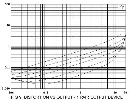
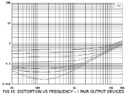
Figure 9 shows the distortion versus power into 8 ohms at 1 KHz, with the lowest curve showing the 1/1 ratio (push pull operation) and the highest curve showing a 0/1 ratio (P2 fully counterclockwise) where Q3 operates as a constant current source and the circuit is operated as singleended Class A.
Figure 10 shows the distortion versus frequency at 1 watt, and we see that the differences between the two settings tends to go away at the highest frequencies, where the variations in capacitance of the devices does not tend to cancel. Also, there are some harmonic content differences over the range of settings. The lowest distortion curves have greater content of higher order harmonics, which tend to go away as you move toward single-ended operation.
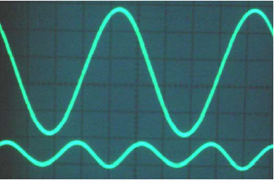
Photo 2 shows an example of the harmonic content with the ratio of top/bottom gain of 2/3, which was one of my favorite settings:
I suggest that you mount P2 on the front panel of the amplifier, and listen to it at the various values. Over most of the range, the open loop gain of the amplifier does not alter significantly until you get close to the counter clockwise position (0/1), where it drops off about 5 dB, resulting about 5 dB of negative feedback. At the 1/1 position, the open loop gain is about 26 dB, giving about 10 dB of feedback. Note that the differences you will hear are not strictly feedback related, but are also a function of push-pull cancellation of distortion.
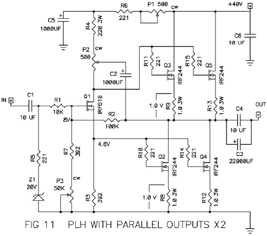
When the amount of power and heat starts getting big, we often parallel output devices in a circuit in order to share the dissipation. In this case the dissipation is about 40 watts per device, and it is tempting to use another pair of devices in parallel with the originals to take that value down to a more reliable 20 watts per device. Figure 11 shows the circuit that does this. Note that I have increased the values of the Source resistors to 1.0 ohm.
PHOTO 2 DISTORTION WAVEFORM @ 1 WATT @ 1 KHZ
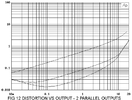
Figure 12 shows the performance of this circuit with the 1/1 setting being the lowest curve, the 0/1 setting the highest, and a 2/3 ratio shown in the middle. There is somewhat less distortion than the curves of Figure 9.
Figure 13 has a little bit different story to tell. At 1 watt over the audio band, the 1/1 ratio might not be considered the best choice, as the 2/3 value has a more uniform performance.
The question often comes up, “How many output devices in parallel is optimal?” The best answer often lies in trial and error. I built a version with 4 parallel devices and 2.0 ohm Source resistors. After measurement and listening, I decided that 4 pairs were too many.
It’s interesting to look at a casual comparison of the results with the original JLH, PLH and two of the Zen amplifiers in the context of simplicity, gain, and feedback applied. All of the amplifiers make it up to 10 watts before the distortion becomes too complex, and they all decline at lower wattages with the second harmonic characteristic described earlier. It’s reasonable to pick 1 watt and 10 watts into 8 ohms as benchmarks. For the PLH example, I used the circuit of Figure 11 with the 1/1 setting.
The greater amount of feedback on some amplifiers helps them to measure better, so we would assume that an otherwise equal amplifier would have some proportionality between measurement and feedback. I was curious about this – If it were true, then how would these amplifiers measure if they all had the same amount of feedback?
I normalized the output impedance and distortion figures to what we would expect if all the amplifiers had 20 dB of feedback and assumed that the difference would be due to feedback:
Gain
Open Loop
Feedback
Zout
Normalized
THD %
Normalized
THD %
Normalized
(dB)
(dB)
(dB)
ohms
ohms
@ 1 Watt
@ 1 Watt
@ 10 Watt
@ 10 Watt
JLH
22
55
33
0.23
1.03
0.03t
0.13
0.12
0.54
ZEN
9
23
15
1.00
0.53
0.60
0.32
2.50
1.33
ZV4
13
33
20
0.60
0.60
0.06
0.06
0.20
0.20
PLH
17
27
10
3.00
0.95
0.04
0.01
0.35
0.11
Here we can see some interesting things. First, for unknown reasons the normalized output impedances of the JLH and PLH are about twice that of the Zen amps.
Second, we see that the original Zen amp stands out as having the highest distortion. This is partially explainable by the fact that the other three designs all have some mechanism to cancel some distortion without negative feedback. In the JLH and PLH, the output stages are driven out of phase by a phase splitter, and in the ZV4 (Zen Variations #4), the P channel input buffer and Aleph current source offer some cancellation.
While the distortion numbers for the JLH are better than the PLH, is operates at about 23 dB more negative feedback. Normalizing these numbers to a 20 dB feedback figure, the PLH appears at least 4 times more linear. Of the potential explanations, the first is the possibility that the more heavily biased Mosfets are more linear the Bipolar devices.
Another possibility is that the input device of the JLH, used to create much of the feedback, is contributing significantly to the distortion. It could be that the data is in error (like that’s never happened), or perhaps the calculation assumption that the distortion would be inversely proportional to the negative feedback is flawed. Maybe it’s all these things.
Now For Something Completely Different
Somewhere in last 26 articles, I grew tired of telling the readers how wonderful it sounds.
So I decided not to do that anymore.
If you want to know, go build it.
Comments and questions are best directed to the Pass Labs forum on www.diyaudio.com
Copyright 2005 Nelson Pass